(→Symbols) |
|||
| Line 24: | Line 24: | ||
Sometimes a fourth terminal for the body (B) is show. In discrete MOSFETs, the body lead is connected internally to the source. When that's the case, the body is also omitted from the symbol. When the bulk is shown, it is sometimes sometimes angled to meet up with the source. In ICs with a common bulk, the bulk is typically not shown and instead an inverting bubble is used to represent a PMOS. | Sometimes a fourth terminal for the body (B) is show. In discrete MOSFETs, the body lead is connected internally to the source. When that's the case, the body is also omitted from the symbol. When the bulk is shown, it is sometimes sometimes angled to meet up with the source. In ICs with a common bulk, the bulk is typically not shown and instead an inverting bubble is used to represent a PMOS. | ||
| − | {| class="wikitable | + | {| class="wikitable" |
|- | |- | ||
! rowspan="2" | Channel !! colspan="2" | Depletion MOSFET !! colspan="2" | Enhancement MOSFT | ! rowspan="2" | Channel !! colspan="2" | Depletion MOSFET !! colspan="2" | Enhancement MOSFT | ||
Revision as of 02:39, 22 March 2014
MOSFET (Metal-Oxide-Semiconductor Field-Effect-Transistor) is a type of Field-effect transistor which utilizes an insulator (such as SiO2) between the gate and the body. Today, MOSFET is the most common type of transistor for both digital and analog circuits.
Overview
The basic starting material for most integrated circuits based on MOSFET technology is typically Silicon (Si); though other processes such as silicon-germanium (Si1−xGex) also exist. Silicon is a very brittle metalloid. It has the same structure as a diamond in elemental form (the actual structure is a 3D tetrahedral, just like carbon). It's a Group IV element - each silicon forming single covalent bonds with four adjacent silicon atoms. Because all of its valence electrons are involved in chemical bonds, pure silicon is quite a poor conductor of electricity. It's possible to raise the conductivity of silicon by introducing impurities, known as dopants, into the silicon lattice through a processes known as doping. Similar results can also be achieved by adding group V elements (which have 5 bonding electrons vs 4 for Si) such as phosphorus or arsenic. By inserting those group V elements into the silicon lattice it can still bond to the 4 original silicon atoms neighbors. The 5th valence electron is loosely bound to that group V element. The thermal vibrations is enough make that electron free to move - leaving positive ions and a free electron. It is this free electron that can carry current thereby increasing the conductivity of the lattice. The process forms a new semiconductor called an n-type semiconductor. The processes can be done with a group III element as well. This creates a situation where each atom is now short by an electron. The missing electron (or hole) propagates about the lattice. The hole acts as a positive carrier gaining the name p-type semiconductor.
A diode is the junction between p-type semiconductors and n-type semiconductors. When the voltage on the p-type semiconductors, known as anode, is raised above the n-type semiconductors, known as a cathode, the diode is said to be forward biased. When that happens, current flows. When the anode voltage is equal to or less than the cathode voltage, the diode is reverse biased - at which point very little current flows. Varying the voltage between the gate and body modulates the conductivity of this layer effectively controlling the current flow between drain and source.
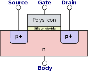
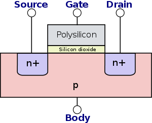
MOS sandwich-like structure is created by superimposing several layers of conducting and insulating together. The actual process involves oxidation of the silicon, doping of the silicon using dopants, and etching of metal wires and contacts. Transistors are built on a pure and flawless single crystals of silicon. Each transistor consists of a body - the silicon wafer. The body is often grounded, often considered the reference node. Each transistor has a stack of the conducting gate that sits on top of an isolating glass (SiO2), and the substrate (also known as the body). Because originally the gate was made from metal, the name metal-oxide semiconductor (MOS) got stuck. Today, the gates are made of polysilicon (Short for polycrystalline sillicon).
An nMOS transistor is built with a p-type body with two regions of n-type semiconductor adjacent to the gate called the source and the drain. For all practical purposes they are physically equivalent and can be used interchangeably. A pMOS transistor is built with an n-type body with two regions of p-type semiconductors adjacent to the gate. Both pMOS and nMOS have a controlling gate. The controlling gate, as the name implies, controls the flow of electrons between the source and drain. In the nMOS transistor, since the body is grounded, the p-n junctions of the source and drain to body are reverse-biased. If the voltage at the gate is raised, an electric field starts to build up - attracting free electrons to the underside of the Si-SiO2 interface. When the voltage is high enough, the electrons end up filling all the holes and a thin region under the gate called the channel gets inverted to act as an n-type semiconductor - creating a conducting path from the source to the drain, allowing current to flow. When the transistor is at that state, we say the transistor is ON. If the gate is grounded, little to no current flows through the reverse-biased junction. When that happens, we say the transistor is OFF.
In the pMOS transistor, the behavior and setup is the complement of the nMOS transistor. The body is held at positive voltage. When the gate is also positive - the source and drain are reverse-biased. When that happens, no current flows and we say the transistor is OFF.
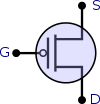
When the voltage at the gate is lowered, positive charges are attracted to the underside of the Si-SiO2 interface. When the voltage gets sufficiently low the channel gets inverted - creating a conducting path from the source to the drain, allowing current to flow. Because the behavior of a pMOS transistor is the opposite of that of an nMOS transistor, the symbol for pMOS transistor is identical to that of nMOS with an additional bubble on the gate. That bubble is known as an inversion bubble.
When dealing with digital logic there are generally only have two distinct values - ON and OFF, 1 and 0, or HIGH and LOW. The positive voltage of the transistor is called VDD (or POWER or PWR). VDD represents the logic 1 value in digital circuits. In TTL logic, the VDD voltage levels were usually around 5 volts. Today's transistors cannot really withstand such high voltages - they are typically in the 1.5V to 3.3V range. The low voltage is often called GROUND (or GND or VSS). VSS represents the logic 0. It is also normally set to 0 volts.
Symbols
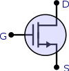
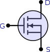
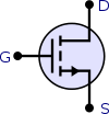
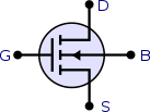
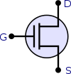
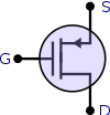
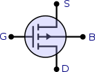
There is no one standard that is commonly accepted across all organizations. Typically individual design groups adopt their own notations. Generally speaking, however, most follow the designs shown below which consists of a lone for the channel with the source and drain leaving it at right angles and then bending back at right angles outwards. Each device has a gate (G), drain (D), and a source (S), A distinction is sometimes made for enhancement mode where the channel is broken down into three smaller lines; it is sometimes drawn as a dotted line instead as well. Depletion mode devices have a solid line instead, this is due to the channel existing prior to power being applied.
Sometimes a fourth terminal for the body (B) is show. In discrete MOSFETs, the body lead is connected internally to the source. When that's the case, the body is also omitted from the symbol. When the bulk is shown, it is sometimes sometimes angled to meet up with the source. In ICs with a common bulk, the bulk is typically not shown and instead an inverting bubble is used to represent a PMOS.
| Channel | Depletion MOSFET | Enhancement MOSFT | ||
|---|---|---|---|---|
| W/ bulk | W/O bulk | W/ bulk | W/O bulk | |
| N-type | 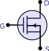 |
 |
 |
|
 |
 |
| ||
| P-type |  |
 |
 |

|
 |
 |
| ||

