From WikiChip
Difference between revisions of "intel/microarchitectures/broadwell (client)"
| Line 42: | Line 42: | ||
| extension 15 = RDRND | | extension 15 = RDRND | ||
| extension 16 = FMA | | extension 16 = FMA | ||
| − | | extension 17 = | + | | extension 17 = F16C |
| − | | extension 18 = | + | | extension 18 = BMI |
| − | | extension 19 = | + | | extension 19 = BMI2 |
| − | | extension 20 = RDSEED | + | | extension 20 = VT-x |
| − | | extension | + | | extension 21 = VT-d |
| − | | extension | + | | extension 22 = TXT |
| + | | extension 22 = TSX | ||
| + | | extension 23 = RDSEED | ||
| + | | extension 24 = ADCX | ||
| + | | extension 25 = PREFETCHW | ||
| cache = Yes | | cache = Yes | ||
Revision as of 22:53, 13 April 2016
| Edit Values | |
| Broadwell µarch | |
| General Info |
Broadwell (BDW) is Intel's microarchitecture based on the 14 nm process for mobile, desktops, and servers. Introduced in early 2015, Broadwell is a process shrink of Haswell which introduced several enhancements. Broadwell is named after Broadwell, Illinois.
Contents
Codenames
| Core | Abbrev | Target |
|---|---|---|
| Broadwell Y | BDW-Y | Core M family, SoC for Smartphones, 2-in-1s Tablets, and notebooks |
| Broadwell U | BDW-U | Core ultrabooks |
| Broadwell H | BDW-H | IoT (QM87, HM86/HM87 Chipsets), All-in-ones |
| Broadwell DT | BDW-DT | Unlocked desktop MPUs |
| Broadwell EP | BDW-EP | Xeon E5, Dual-Processor platform |
| Broadwell EX | BDW-EX | Xeon E5, Multi-Processor platform, QPI |
| Broadwell E | BDW-E | High-End Desktops (HEDT) |
Architecture
Broadwell is for the most part identical to Haswell with several enhancements.
Key changes from Haswell
- ~5% IPC improvement
- FP multiplication instructions has reduced latency (3 cycles, down from 5)
- Affects AVX, SSE, and FP instructions
- CLMUL instructions are now a single μop, improving latency and throughput
- The second-level TLB (STLB)
- Table was enlarged (1,536 entries, up from 1024)
- 1GB page mode (16 entries, 4-ways set associative)
- Larger out-of-order scheduler
- Faster store-to-load forwarding
- Address prediction for branches and returns was improved
- Improved cryptography acceleration instructions
Core features maintained a 2:1 ratio of performance:power.
Graphics
- 50% higher sampler throughput
- Improvements for increased geometry, Z, Pixel Fill
- Direct X 11.2, OpenGL 4.3
- OpenCL 1.2 and 2.0 (with Shared Virtual Memory)
- Up to 24 EUs (20% addition, up from 20 in Haswell), 48 EUs on Iris Pro Graphics
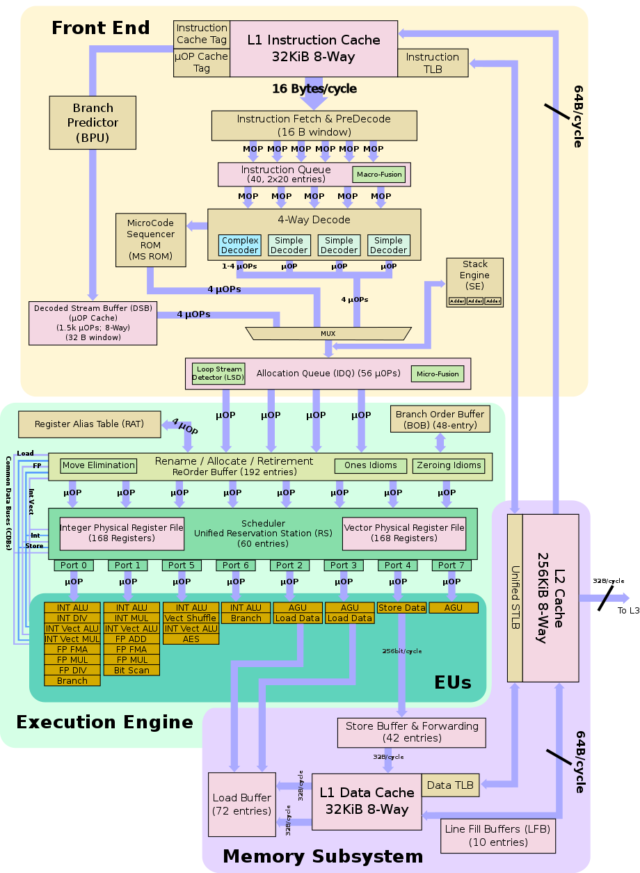
Block Diagram
Memory Hierarchy
- Cache
- Hardware prefetchers
- L1 Cache:
- 32 KB 8-way set associative instruction, 64 B line size
- 32 KB 8-way set associative data, 64 B line size
- Write-back policy
- Per core
- L2 Cache:
- 256 KB 8-way set associative, 64 B line size
- Write-back policy
- Per core
- L3 Cache:
- 1.5 MB
- L4 Cache:
- 128 MB
- eDRAM
- shared with GPU (Crystal Well)
- Iris Pro models only
