Semiconductor & Computer Engineering
(→Alder Lake S Processors) |
(fixed) |
||
| (One intermediate revision by one other user not shown) | |||
| Line 9: | Line 9: | ||
|microarch=Alder Lake | |microarch=Alder Lake | ||
|word=64 bit | |word=64 bit | ||
| − | |proc=Intel 7 | + | |proc=10 nm |
| + | |proc 2=7 nm <!-- Intel 7 --> | ||
|tech=CMOS | |tech=CMOS | ||
|predecessor=Rocket Lake S | |predecessor=Rocket Lake S | ||
| − | |predecessor link=intel/cores/rocket lake | + | |predecessor link=intel/cores/rocket lake s |
|successor=Raptor Lake S | |successor=Raptor Lake S | ||
|successor link=intel/cores/raptor lake s | |successor link=intel/cores/raptor lake s | ||
}} | }} | ||
| − | '''Alder Lake S''' ( | + | |
| + | '''Alder Lake S''' (''ADL-S'') is the name of [[Intel]]'s mainstream performance line of processors based on the {{intel|Alder Lake|Alder Lake microarchitecture|l=arch}} serving as a successor to {{\\|Rocket Lake S}}. These chips are primarily targeted towards desktop performance to value computers, AiOs, and minis. Alder Lake S processors are fabricated on [[Intel 7]] process. Alder Lake S is the first series of mainstream desktop heterogeneous multi-core microprocessors from [[Intel]]. | ||
==Overview== | ==Overview== | ||
| − | Alder Lake S based processors are a 2-chip solution - the microprocessor and the chipset. Alder Lake S utilize Socket LGA-1700 and use 600-series chipset (HUB). The microprocessor is connected to the chipset via 8 of the chip's 28 PCIe lanes using Intel's proprietary Direct Media Interface 4.0 (DMI 4.0), allowing for 16 GT/s transfer rate per lane. | + | '''Alder Lake S''' based processors are a 2-chip solution - the microprocessor and the chipset. Alder Lake S utilize Socket LGA-1700 and use 600-series chipset ([[HUB]]). The microprocessor is connected to the chipset via 8 of the chip's 28 PCIe lanes using [[Intel]]'s proprietary ''Direct Media Interface'' 4.0 ([[DMI]] 4.0), allowing for 16 GT/s transfer rate per lane. |
=== Common Features === | === Common Features === | ||
| Line 25: | Line 27: | ||
* Dual-channel Memory | * Dual-channel Memory | ||
| − | ** DDR4-3200 | + | ** DDR4-3200 or DDR5-4800 |
| − | ** 128 GiB | + | ** 128 GiB memory |
* 20x PCIe Lanes | * 20x PCIe Lanes | ||
** 16x PCIe 5.0 (for discrete graphics) | ** 16x PCIe 5.0 (for discrete graphics) | ||
** 4x PCIe 4.0 (for storage) | ** 4x PCIe 4.0 (for storage) | ||
* [[6 cores|6]]-[[16 cores|16]] cores | * [[6 cores|6]]-[[16 cores|16]] cores | ||
| − | * Everything up to AVX2 (SMM, FPU, NX, MMX, SSE, SSE2, SSE3, SSSE3, SSE4.1, SSE4.2, AES, AVX, FMA3, and AVX2) | + | * Everything up to AVX2 (SMM, FPU, NX, MMX, SSE, SSE2, SSE3, SSSE3, |
| + | :SSE4.1, SSE4.2, AES, AVX, FMA3, and AVX2) | ||
* Graphics | * Graphics | ||
| − | ** Xe Graphics ({{intel|Gen12|l=arch}}) {{intel|UHD Graphics 770}} (GT2) | + | ** Xe Graphics ({{intel|Gen12|l=arch}}) {{intel|UHD Graphics 770}} (GT2) GPU |
{{clear}} | {{clear}} | ||
| Line 78: | Line 81: | ||
</table> | </table> | ||
{{comp table end}} | {{comp table end}} | ||
| + | |||
| + | == Die == | ||
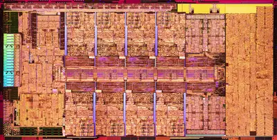
| + | {{main|intel/microarchitectures/alder lake#ADL-S (8P+8E)|l1=Alder Lake § ADL-S (8P+8E) Die}} | ||
| + | Alder Lake S (C0) microprocessors are fabricated on [[Intel]]'s [[Intel 7|Intel 7 process]]. This SoC uses a single 215.25 mm² monolithic die which includes both the CPU cores along with the integrated GPU and various other additional components. | ||
| + | |||
| + | * [[Intel 7|Intel 7 process]] | ||
| + | * 10.5 mm x 20.5 mm | ||
| + | * 215.25 mm² die size | ||
| + | |||
| + | |||
| + | :[[File:alder lake die 2.png|400px|link=intel/microarchitectures/alder lake#ADL-S (8P+8E)]] | ||
== See also == | == See also == | ||
{{intel alder lake core see also}} | {{intel alder lake core see also}} | ||
Latest revision as of 18:56, 1 April 2025
| Edit Values | |
| Alder Lake S | |
| General Info | |
| Designer | Intel |
| Manufacturer | Intel |
| Microarchitecture | |
| ISA | x86-64 (x86) |
| Microarchitecture | Alder Lake |
| Word Size | 8 octets 64 bit16 nibbles |
| Process | 10 nm 0.01 μm , 7 nm1.0e-5 mm 0.007 μm 7.0e-6 mm |
| Technology | CMOS |
| Succession | |
Alder Lake S (ADL-S) is the name of Intel's mainstream performance line of processors based on the Alder Lake microarchitecture serving as a successor to Rocket Lake S. These chips are primarily targeted towards desktop performance to value computers, AiOs, and minis. Alder Lake S processors are fabricated on Intel 7 process. Alder Lake S is the first series of mainstream desktop heterogeneous multi-core microprocessors from Intel.
Overview[edit]
Alder Lake S based processors are a 2-chip solution - the microprocessor and the chipset. Alder Lake S utilize Socket LGA-1700 and use 600-series chipset (HUB). The microprocessor is connected to the chipset via 8 of the chip's 28 PCIe lanes using Intel's proprietary Direct Media Interface 4.0 (DMI 4.0), allowing for 16 GT/s transfer rate per lane.
Common Features[edit]
All Alder Lake S processors have the following:
- Dual-channel Memory
- DDR4-3200 or DDR5-4800
- 128 GiB memory
- 20x PCIe Lanes
- 16x PCIe 5.0 (for discrete graphics)
- 4x PCIe 4.0 (for storage)
- 6-16 cores
- Everything up to AVX2 (SMM, FPU, NX, MMX, SSE, SSE2, SSE3, SSSE3,
- SSE4.1, SSE4.2, AES, AVX, FMA3, and AVX2)
- Graphics
- Xe Graphics (Gen12) UHD Graphics 770 (GT2) GPU
Alder Lake S Processors[edit]
| List of Alder Lake S-based Processors | |||||||||||||
|---|---|---|---|---|---|---|---|---|---|---|---|---|---|
| Main processor | GPU | ||||||||||||
| Model | Launched | Price | Family | Cores | Threads | L3$ | TDP | Frequency | Turbo | Max Mem | Name | Frequency | Turbo |
| i5-12600K | 4 November 2021 | $ 289.00 € 260.10 , $ 299.00£ 234.09 ¥ 29,862.37 € 269.10 £ 242.19 ¥ 30,895.67 | Core i5 | 10 | 16 | 2 MiB 2,048 KiB , 18 MiB2,097,152 B 0.00195 GiB 18,432 KiB 18,874,368 B 0.0176 GiB | 125 W 125,000 mW 0.168 hp 0.125 kW | 3.7 GHz 3,700 MHz 3,700,000 kHz | 128 GiB 131,072 MiB 134,217,728 KiB 137,438,953,472 B 0.125 TiB | UHD Graphics 770 | 300 MHz 0.3 GHz 300,000 KHz | 1,450 MHz 1.45 GHz 1,450,000 KHz | |
| i5-12600KF | 4 November 2021 | $ 264.00 € 237.60 , $ 274.00£ 213.84 ¥ 27,279.12 € 246.60 £ 221.94 ¥ 28,312.42 | Core i5 | 10 | 16 | 2 MiB 2,048 KiB , 18 MiB2,097,152 B 0.00195 GiB 18,432 KiB 18,874,368 B 0.0176 GiB | 125 W 125,000 mW 0.168 hp 0.125 kW | 3.7 GHz 3,700 MHz 3,700,000 kHz | 128 GiB 131,072 MiB 134,217,728 KiB 137,438,953,472 B 0.125 TiB | ||||
| i7-12700K | 4 November 2021 | $ 409.00 € 368.10 , $ 419.00£ 331.29 ¥ 42,261.97 € 377.10 £ 339.39 ¥ 43,295.27 | Core i7 | 12 | 20 | 1 MiB 1,024 KiB , 24 MiB1,048,576 B 9.765625e-4 GiB 24,576 KiB 25,165,824 B 0.0234 GiB | 125 W 125,000 mW 0.168 hp 0.125 kW | 3.6 GHz 3,600 MHz 3,600,000 kHz | 128 GiB 131,072 MiB 134,217,728 KiB 137,438,953,472 B 0.125 TiB | UHD Graphics 770 | 300 MHz 0.3 GHz 300,000 KHz | 1,500 MHz 1.5 GHz 1,500,000 KHz | |
| i7-12700KF | 4 November 2021 | $ 384.00 € 345.60 , $ 394.00£ 311.04 ¥ 39,678.72 € 354.60 £ 319.14 ¥ 40,712.02 | Core i7 | 12 | 20 | 1 MiB 1,024 KiB , 24 MiB1,048,576 B 9.765625e-4 GiB 24,576 KiB 25,165,824 B 0.0234 GiB | 125 W 125,000 mW 0.168 hp 0.125 kW | 3.6 GHz 3,600 MHz 3,600,000 kHz | 128 GiB 131,072 MiB 134,217,728 KiB 137,438,953,472 B 0.125 TiB | ||||
| i9-12900K | 4 November 2021 | $ 589.00 € 530.10 , $ 599.00£ 477.09 ¥ 60,861.37 € 539.10 £ 485.19 ¥ 61,894.67 | Core i9 | 16 | 24 | 6 MiB 6,144 KiB , 24 MiB6,291,456 B 0.00586 GiB 24,576 KiB 25,165,824 B 0.0234 GiB | 125 W 125,000 mW 0.168 hp 0.125 kW | 3.2 GHz 3,200 MHz 3,200,000 kHz | 128 GiB 131,072 MiB 134,217,728 KiB 137,438,953,472 B 0.125 TiB | UHD Graphics 770 | 300 MHz 0.3 GHz 300,000 KHz | 1,550 MHz 1.55 GHz 1,550,000 KHz | |
| i9-12900KF | 4 November 2021 | $ 564.00 € 507.60 , $ 574.00£ 456.84 ¥ 58,278.12 € 516.60 £ 464.94 ¥ 59,311.42 | Core i9 | 16 | 24 | 6 MiB 6,144 KiB , 24 MiB6,291,456 B 0.00586 GiB 24,576 KiB 25,165,824 B 0.0234 GiB | 125 W 125,000 mW 0.168 hp 0.125 kW | 3.2 GHz 3,200 MHz 3,200,000 kHz | 128 GiB 131,072 MiB 134,217,728 KiB 137,438,953,472 B 0.125 TiB | ||||
| Count: 6 | |||||||||||||
Die[edit]
- Main article: Alder Lake § ADL-S (8P+8E) Die
Alder Lake S (C0) microprocessors are fabricated on Intel's Intel 7 process. This SoC uses a single 215.25 mm² monolithic die which includes both the CPU cores along with the integrated GPU and various other additional components.
- Intel 7 process
- 10.5 mm x 20.5 mm
- 215.25 mm² die size
See also[edit]
|
• Power
• Performance |
| designer | Intel + |
| instance of | core + |
| isa | x86-64 + |
| isa family | x86 + |
| manufacturer | Intel + |
| microarchitecture | Alder Lake + |
| name | Alder Lake S + |
| technology | CMOS + |
| word size | 64 bit (8 octets, 16 nibbles) + |