(→Terminology) |
|||
| (4 intermediate revisions by 3 users not shown) | |||
| Line 1: | Line 1: | ||
| − | [[File:mask diagram.svg|thumb|right]][[File:Chromium photomask (details).JPG|thumb|200px|right|A detailed picture of the opaque and transparent patterns on a chromium mask.]] | + | {{title|Mask / Reticle}}[[File:mask diagram.svg|thumb|right]][[File:Chromium photomask (details).JPG|thumb|200px|right|A detailed picture of the opaque and transparent patterns on a chromium mask.]] |
| − | A '''mask''' or '''reticle''' (sometimes '''photomask''' and '''photoreticle''') is pattern transferring device used in the fabrication of microelectronic for pattern transfers. | + | A '''mask''' or '''reticle''' (sometimes '''photomask''' and '''photoreticle''') is a pattern transferring device used in the fabrication of microelectronic for pattern transfers. |
== Overview == | == Overview == | ||
| Line 8: | Line 8: | ||
== Terminology == | == Terminology == | ||
| + | [[File:intel mask.jpg|right|thumb|Modern Intel 6" [[14 nm]]/[[10 nm]] test reticle.]] | ||
Historically, a '''mask''' or '''photomask''' referred to a pattern transferring device that contained the entire pattern of a single layer of a full wafer. A '''reticle''', on the other hand, referred to a single layer of pattern that covers a small portion of the wafer. A reticle has to be stepped and repeated in order to expose the entire wafer. In other words, compared to a reticle, a mask used to refer to a pattern that could be printed in a single exposure to cover the entire wafer without any optical de-magnification. Today, the terms are often used synonymously. | Historically, a '''mask''' or '''photomask''' referred to a pattern transferring device that contained the entire pattern of a single layer of a full wafer. A '''reticle''', on the other hand, referred to a single layer of pattern that covers a small portion of the wafer. A reticle has to be stepped and repeated in order to expose the entire wafer. In other words, compared to a reticle, a mask used to refer to a pattern that could be printed in a single exposure to cover the entire wafer without any optical de-magnification. Today, the terms are often used synonymously. | ||
| Line 23: | Line 24: | ||
== Reticle limit == | == Reticle limit == | ||
| − | Current i193 and [[EUV]] lithography steppers have a maximum field size of 26 mm by 33 mm or 858 mm². | + | Current i193 and [[EUV]] lithography steppers have a maximum field size of 26 mm by 33 mm or 858 mm². In future [[High-NA EUV]] lithography steppers the reticle limit will be halved to 26 mm by 16,5 mm or 429 mm² due to the use of anamorphic lens array. |
==See also== | ==See also== | ||
* [[mask count]] | * [[mask count]] | ||
* [[mask set]] | * [[mask set]] | ||
Latest revision as of 16:17, 29 January 2024
A mask or reticle (sometimes photomask and photoreticle) is a pattern transferring device used in the fabrication of microelectronic for pattern transfers.
Overview[edit]
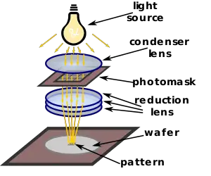
A mask is a pattern transferring device, a glass or fused silica/quartz plate with opaque and transparent patterns on its surface. A mask works much like a negative - by shining light through the mask, the detailed device image can then be projected onto the wafer (see photoresist). The transmitted image is often passed through some sort of lens capable of de-magnifying the images before reaching the receiving substrate.
Each individual mask contains a single pattern which when stacked together forms the common electrical elements such as resistors, capacitors and transistors. An entire mask set is then fed into a photolithography stepper which cycle through the set, exposing individual masks to the wafers to form the circuitry needed.
Terminology[edit]
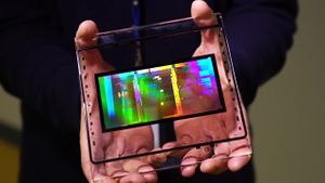
Historically, a mask or photomask referred to a pattern transferring device that contained the entire pattern of a single layer of a full wafer. A reticle, on the other hand, referred to a single layer of pattern that covers a small portion of the wafer. A reticle has to be stepped and repeated in order to expose the entire wafer. In other words, compared to a reticle, a mask used to refer to a pattern that could be printed in a single exposure to cover the entire wafer without any optical de-magnification. Today, the terms are often used synonymously.
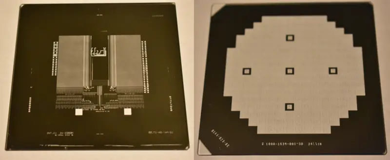
Below is a 5-inch IBM reticle next to a 4-inch AMI Semi photomask.
Manufacturing Process[edit]
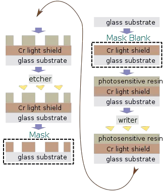
Masks are made using a photomask blank. The mask blanks are made from a finely polished quartz glass which acts as the glass substrate and Chromium atoms which are deposited on top of it to create a light-shielding layer. A coat of photosensitive resin is then used to cover the surface of the mask blank. Using electron beams a circuit pattern is then written onto the mask. Depending on the technique used either the exposed or non-exposed portion of the resist gets removed.
It is during that stage that the mask blank with the writing is finely inspected for quality. If any issues are observed the mask is recycled and gets re-written. If the mask passes inspection the written pattern is then etched. Plasma etching is done via a plasma etcher which sprays ions onto the mask penetration and dissolving the chromium in the exposed areas. Finally the leftover resistant is removed forming the final product - a mask with transparent and opaque patterns.
Reticle limit[edit]
Current i193 and EUV lithography steppers have a maximum field size of 26 mm by 33 mm or 858 mm². In future High-NA EUV lithography steppers the reticle limit will be halved to 26 mm by 16,5 mm or 429 mm² due to the use of anamorphic lens array.


