(→Graphics) |
|||
| (30 intermediate revisions by 4 users not shown) | |||
| Line 2: | Line 2: | ||
{{core | {{core | ||
|name=Kaby Lake G | |name=Kaby Lake G | ||
| − | | | + | |image=kaby lake g (front).png |
| + | |caption=Package front | ||
|developer=Intel | |developer=Intel | ||
|developer 2=AMD | |developer 2=AMD | ||
| Line 8: | Line 9: | ||
|manufacturer 2=GlobalFoundries | |manufacturer 2=GlobalFoundries | ||
|first announced=November 6, 2017 | |first announced=November 6, 2017 | ||
| + | |first launched=January 7, 2018 | ||
|isa=x86-64 | |isa=x86-64 | ||
|isa family=x86 | |isa family=x86 | ||
| Line 15: | Line 17: | ||
|tech=CMOS | |tech=CMOS | ||
}} | }} | ||
| − | '''Kaby Lake G''' ('''KBL-G''') is the name of the core for [[Intel]]'s high-performance line of mobile processors based on the {{intel|Kaby Lake|l=arch}} microarchitecture | + | '''Kaby Lake G''' ('''KBL-G''') is the name of the core for [[Intel]]'s high-performance line of mobile processors based on the {{intel|Kaby Lake|l=arch}} microarchitecture and incorporate a discrete [[AMD]] {{amd|Vega|l=arch}} graphics processor. These chips are targeted towards ultimate mobile gaming experience. Kaby Lake G processors are fabricated on Intel's enhanced [[14 nm lithography process|14nm+ process]] and for graphics, GlobalFoundries [[14 nm process]]. |
| + | == Overview == | ||
| + | [[File:8th gen core i7 with radeon logo (2018).png|250px|right]] | ||
| + | [[File:8th gen core i5 with radeon logo (2018).png|250px|right]] | ||
| + | {{see also|intel/microarchitectures/kaby_lake#Kaby_Lake_G|l1=Kaby Lake § Kaby Lake G}} | ||
| + | Kaby Lake G based processors are a 2-chip solution - the [[microprocessor]] and the [[chipset]]. Those parts are [[BGA]] and are soldered onto the motherboard. The microprocessor is connected to the chipset via 4 of the chip's 20 PCIe lanes using Intel's proprietary {{intel|Direct Media Interface}} 3.0 (DMI 3.0), allowing for 8 GT/s transfer rate per lane. The microprocessor itself is identical to one used for the {{intel|Kaby Lake H|l=core}} but is now packaged along with the Radeon GPU and [[HBM 2]]. | ||
| − | {{ | + | === Graphics === |
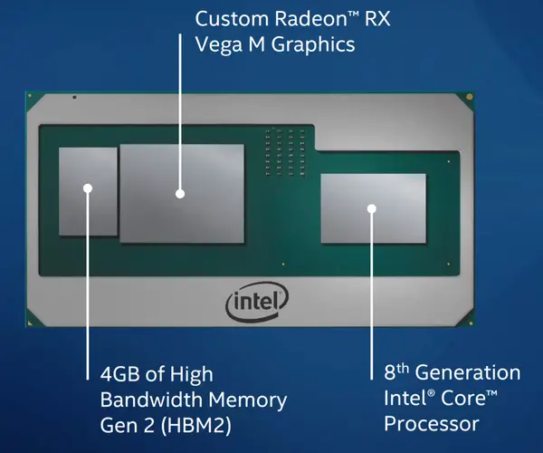
| + | Those processors are unique in the fact that this is the first time Intel has integrated a discrete graphics processor into the same package as the microprocessor. This is also the first time they are using a competitor's graphics processor. Those parts incorporate an [[AMD]] [[GPU]] based on the {{amd|Vega|l=arch}} microarchitecture and incorporate their own 4 GiB of [[high-bandwidth memory]] 2 (HBM2). The HBM solution is connected to the graphics processor using Intel's [[EMIB]], a high-speed in-package interconnect solution. | ||
| + | The CPU itself is connected to the GPU using 8 of the other PCIe lanes, leaving the 8 remaining lanes for other peripherals to communicate with the CPU directly. | ||
| − | + | ||
| − | + | [[File:kaby lake g with amd radeon package.png|600px]] | |
=== Common Features === | === Common Features === | ||
| Line 30: | Line 39: | ||
** Up to DDR3L-1600, DDR4-2400 | ** Up to DDR3L-1600, DDR4-2400 | ||
** Up to 64 GiB | ** Up to 64 GiB | ||
| − | * 8x PCIe | + | * 8x PCIe |
| + | ** 20x in total, 4 of the 20 are used by the bus and 8 for the GPU as described above | ||
* [[quad-core]] with {{intel|Hyper-Threading}} (8 threads) | * [[quad-core]] with {{intel|Hyper-Threading}} (8 threads) | ||
* Everything up to AVX2 (SMM, FPU, NX, MMX, SSE, SSE2, SSE3, SSSE3, SSE4.1, SSE4.2, AES, AVX, and AVX2) | * Everything up to AVX2 (SMM, FPU, NX, MMX, SSE, SSE2, SSE3, SSSE3, SSE4.1, SSE4.2, AES, AVX, and AVX2) | ||
| + | * BGA package | ||
| + | |||
| + | ==== Graphics ==== | ||
| + | [[File:kbl-g graphics subsystem.png|thumb|right|400px|Graphics Subsystem]] | ||
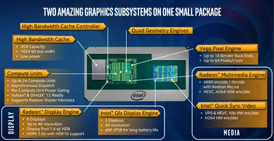
| + | Those processors have superior graphics capabilities as well as 4 GiB of [[HBM 2]] cache. | ||
| + | |||
| + | * [[HBM 2]] (Intel calls "High Bandwidth Cache" or "HBC") | ||
| + | ** 4 GiB | ||
| + | ** 1,024 bit | ||
| + | *** @ 800 MHz (204.8 GB/s peak bandwidth) | ||
| + | *** @ 700 MHz (179.2 GB/s peak bandwidth) | ||
* Graphics | * Graphics | ||
| + | ** 9 Display outputs available | ||
** Integrated {{intel|HD Graphics 630}} ({{intel|Gen9.5|l=arch}} GT2) | ** Integrated {{intel|HD Graphics 630}} ({{intel|Gen9.5|l=arch}} GT2) | ||
| + | *** 3 Displays | ||
*** Base frequency of 350 MHz | *** Base frequency of 350 MHz | ||
| − | *** Burst frequency of 1. | + | *** Burst frequency of 1.1 GHz |
| − | ** Discrete {{amd|Vega|l=arch}} | + | ** Discrete {{amd|Vega|l=arch}}-based GPUs |
| − | *** | + | *** Custom Radeon RX Vega M Graphics |
| + | **** 6 Displays | ||
| + | **** [[Radeon RX Vega M GH]] | ||
| + | ***** 24 Compute Units | ||
| + | ***** 1,536 Stream processors, 64 pix/clk (ROPs), 96 texture units | ||
| + | ***** 3.7 TFLOPS peak performance | ||
| + | **** [[Radeon RX Vega M GL]] | ||
| + | ***** 20 Compute Units | ||
| + | ***** 1,280 Stream processors, 32 pix/clk (ROPs), 80 texture units | ||
| + | ***** 2.6 TFLOPS peak performance | ||
{{clear}} | {{clear}} | ||
| − | |||
== Kaby Lake G Processors == | == Kaby Lake G Processors == | ||
| Line 52: | Line 83: | ||
--> | --> | ||
{{comp table start}} | {{comp table start}} | ||
| − | <table class="comptable sortable tc4"> | + | <table class="comptable sortable tc4 tc5 tc13 tc14"> |
| − | {{comp table header|main| | + | {{comp table header|main|13:List of Kaby Lake G-based Processors}} |
| − | {{comp table header|main| | + | {{comp table header|main|8:Main processor|3:Graphics Processors|2:Features}} |
| − | {{comp table header|cols | + | {{comp table header|cols|Launched|Family|C|T|L3$|TDP|%Frequency|%Turbo|GPU|Base|Burst|vPro|Locked}} |
{{#ask: [[Category:microprocessor models by intel]] [[instance of::microprocessor]] [[core name::Kaby Lake G]] | {{#ask: [[Category:microprocessor models by intel]] [[instance of::microprocessor]] [[core name::Kaby Lake G]] | ||
|?full page name | |?full page name | ||
|?model number | |?model number | ||
|?first launched | |?first launched | ||
| − | |||
|?microprocessor family | |?microprocessor family | ||
|?core count | |?core count | ||
| Line 71: | Line 101: | ||
|?integrated gpu base frequency | |?integrated gpu base frequency | ||
|?integrated gpu max frequency | |?integrated gpu max frequency | ||
| + | |?has intel vpro technology | ||
| + | |?has locked clock multiplier | ||
|format=template | |format=template | ||
|template=proc table 3 | |template=proc table 3 | ||
| − | |userparam=14 | + | |userparam=15:14 |
|mainlabel=- | |mainlabel=- | ||
|valuesep=, | |valuesep=, | ||
Latest revision as of 18:07, 12 July 2018
| Edit Values | |
| Kaby Lake G | |
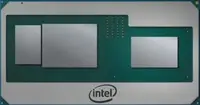 | |
| Package front | |
| General Info | |
| Designer | Intel, AMD |
| Manufacturer | Intel, GlobalFoundries |
| Introduction | November 6, 2017 (announced) January 7, 2018 (launched) |
| Microarchitecture | |
| ISA | x86-64 (x86) |
| Microarchitecture | Kaby Lake |
| Word Size | 8 octets 64 bit16 nibbles |
| Process | 14 nm 0.014 μm 1.4e-5 mm |
| Technology | CMOS |
Kaby Lake G (KBL-G) is the name of the core for Intel's high-performance line of mobile processors based on the Kaby Lake microarchitecture and incorporate a discrete AMD Vega graphics processor. These chips are targeted towards ultimate mobile gaming experience. Kaby Lake G processors are fabricated on Intel's enhanced 14nm+ process and for graphics, GlobalFoundries 14 nm process.
Contents
Overview[edit]
- See also: Kaby Lake § Kaby Lake G
Kaby Lake G based processors are a 2-chip solution - the microprocessor and the chipset. Those parts are BGA and are soldered onto the motherboard. The microprocessor is connected to the chipset via 4 of the chip's 20 PCIe lanes using Intel's proprietary Direct Media Interface 3.0 (DMI 3.0), allowing for 8 GT/s transfer rate per lane. The microprocessor itself is identical to one used for the Kaby Lake H but is now packaged along with the Radeon GPU and HBM 2.
Graphics[edit]
Those processors are unique in the fact that this is the first time Intel has integrated a discrete graphics processor into the same package as the microprocessor. This is also the first time they are using a competitor's graphics processor. Those parts incorporate an AMD GPU based on the Vega microarchitecture and incorporate their own 4 GiB of high-bandwidth memory 2 (HBM2). The HBM solution is connected to the graphics processor using Intel's EMIB, a high-speed in-package interconnect solution.
The CPU itself is connected to the GPU using 8 of the other PCIe lanes, leaving the 8 remaining lanes for other peripherals to communicate with the CPU directly.
Common Features[edit]
All Kaby Lake G processors have the following:
- Dual-channel Memory
- Up to DDR3L-1600, DDR4-2400
- Up to 64 GiB
- 8x PCIe
- 20x in total, 4 of the 20 are used by the bus and 8 for the GPU as described above
- quad-core with Hyper-Threading (8 threads)
- Everything up to AVX2 (SMM, FPU, NX, MMX, SSE, SSE2, SSE3, SSSE3, SSE4.1, SSE4.2, AES, AVX, and AVX2)
- BGA package
Graphics[edit]
Those processors have superior graphics capabilities as well as 4 GiB of HBM 2 cache.
- HBM 2 (Intel calls "High Bandwidth Cache" or "HBC")
- 4 GiB
- 1,024 bit
- @ 800 MHz (204.8 GB/s peak bandwidth)
- @ 700 MHz (179.2 GB/s peak bandwidth)
- Graphics
- 9 Display outputs available
- Integrated HD Graphics 630 (Gen9.5 GT2)
- 3 Displays
- Base frequency of 350 MHz
- Burst frequency of 1.1 GHz
- Discrete Vega-based GPUs
- Custom Radeon RX Vega M Graphics
- 6 Displays
- Radeon RX Vega M GH
- 24 Compute Units
- 1,536 Stream processors, 64 pix/clk (ROPs), 96 texture units
- 3.7 TFLOPS peak performance
- Radeon RX Vega M GL
- 20 Compute Units
- 1,280 Stream processors, 32 pix/clk (ROPs), 80 texture units
- 2.6 TFLOPS peak performance
- Custom Radeon RX Vega M Graphics
Kaby Lake G Processors[edit]
| List of Kaby Lake G-based Processors | |||||||||||||
|---|---|---|---|---|---|---|---|---|---|---|---|---|---|
| Main processor | Graphics Processors | Features | |||||||||||
| Model | Launched | Family | C | T | L3$ | TDP | Frequency | Turbo | GPU | Base | Burst | vPro | Locked |
| i5-8305G | 7 January 2018 | Core i5 | 4 | 8 | 6 MiB 6,144 KiB 6,291,456 B 0.00586 GiB | 65 W 65,000 mW 0.0872 hp 0.065 kW | 2.8 GHz 2,800 MHz 2,800,000 kHz | 3.8 GHz 3,800 MHz 3,800,000 kHz | HD Graphics 630, Radeon RX Vega M GL | 350 MHz 0.35 GHz , 931 MHz350,000 KHz 0.931 GHz 931,000 KHz | 1,100 MHz 1.1 GHz , 1,011 MHz1,100,000 KHz 1.011 GHz 1,011,000 KHz | ✘ | ✔ |
| i7-8705G | 7 January 2018 | Core i7 | 4 | 8 | 8 MiB 8,192 KiB 8,388,608 B 0.00781 GiB | 65 W 65,000 mW 0.0872 hp 0.065 kW | 3.1 GHz 3,100 MHz 3,100,000 kHz | 4.1 GHz 4,100 MHz 4,100,000 kHz | HD Graphics 630, Radeon RX Vega M GL | 350 MHz 0.35 GHz , 931 MHz350,000 KHz 0.931 GHz 931,000 KHz | 1,100 MHz 1.1 GHz , 1,011 MHz1,100,000 KHz 1.011 GHz 1,011,000 KHz | ✘ | ✔ |
| i7-8706G | 7 January 2018 | Core i7 | 4 | 8 | 8 MiB 8,192 KiB 8,388,608 B 0.00781 GiB | 65 W 65,000 mW 0.0872 hp 0.065 kW | 3.1 GHz 3,100 MHz 3,100,000 kHz | 4.1 GHz 4,100 MHz 4,100,000 kHz | HD Graphics 630, Radeon RX Vega M GL | 350 MHz 0.35 GHz , 931 MHz350,000 KHz 0.931 GHz 931,000 KHz | 1,100 MHz 1.1 GHz , 1,011 MHz1,100,000 KHz 1.011 GHz 1,011,000 KHz | ✔ | ✔ |
| i7-8709G | 7 January 2018 | Core i7 | 4 | 8 | 8 MiB 8,192 KiB 8,388,608 B 0.00781 GiB | 100 W 100,000 mW 0.134 hp 0.1 kW | 3.1 GHz 3,100 MHz 3,100,000 kHz | 4.1 GHz 4,100 MHz 4,100,000 kHz | HD Graphics 630, Radeon RX Vega M GH | 350 MHz 0.35 GHz , 1,063 MHz350,000 KHz 1.063 GHz 1,063,000 KHz | 1,100 MHz 1.1 GHz , 1,190 MHz1,100,000 KHz 1.19 GHz 1,190,000 KHz | ✘ | ✔ |
| i7-8809G | 7 January 2018 | Core i7 | 4 | 8 | 8 MiB 8,192 KiB 8,388,608 B 0.00781 GiB | 100 W 100,000 mW 0.134 hp 0.1 kW | 3.1 GHz 3,100 MHz 3,100,000 kHz | 4.2 GHz 4,200 MHz 4,200,000 kHz | HD Graphics 630, Radeon RX Vega M GH | 350 MHz 0.35 GHz , 1,063 MHz350,000 KHz 1.063 GHz 1,063,000 KHz | 1,100 MHz 1.1 GHz , 1,190 MHz1,100,000 KHz 1.19 GHz 1,190,000 KHz | ✘ | ✘ |
| Count: 5 | |||||||||||||
See also[edit]
|
• Power
• Performance |
| designer | Intel + and AMD + |
| first announced | November 6, 2017 + |
| first launched | January 7, 2018 + |
| instance of | core + |
| isa | x86-64 + |
| isa family | x86 + |
| main image | 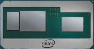 + + |
| main image caption | Package front + |
| manufacturer | Intel + and GlobalFoundries + |
| microarchitecture | Kaby Lake + |
| name | Kaby Lake G + |
| process | 14 nm (0.014 μm, 1.4e-5 mm) + |
| technology | CMOS + |
| word size | 64 bit (8 octets, 16 nibbles) + |
