From WikiChip
Difference between revisions of "renesas/r-car/h3"
(→Cache) |
|||
| (10 intermediate revisions by 3 users not shown) | |||
| Line 1: | Line 1: | ||
{{renesas title|R-Car H3}} | {{renesas title|R-Car H3}} | ||
| − | {{ | + | {{chip |
|name=R-Car H3 | |name=R-Car H3 | ||
|image=r-car h3.png | |image=r-car h3.png | ||
| Line 24: | Line 24: | ||
|process=16 nm | |process=16 nm | ||
|technology=CMOS | |technology=CMOS | ||
| + | |die area=111.36 mm² | ||
| + | |die length=12.94 mm | ||
| + | |die width=8.61 mm | ||
|word size=64 bit | |word size=64 bit | ||
|core count=9 | |core count=9 | ||
| Line 32: | Line 35: | ||
|package module 1={{packages/renesas/fcbga-1384}} | |package module 1={{packages/renesas/fcbga-1384}} | ||
}} | }} | ||
| − | '''R-Car H3''' is a {{arch|64}} [[nona-core]] [[ARM]] SoC designed by [[Renesas]] for the automotive industry and introduced in 2016. The H3 incorporates four {{armh|Cortex-A57}} cores, four {{armh|Cortex-A53}} cores, and a | + | '''R-Car H3''' is a {{arch|64}} [[nona-core]] [[ARM]] SoC designed by [[Renesas]] for the automotive industry and introduced in 2016. The H3 incorporates four {{armh|Cortex-A57}} cores, four {{armh|Cortex-A53}} cores, and a dual-core lock-step {{armh|Cortex-R7}} for real-time processing. This chip supports up to quad-channel LPDDR4-3200 memory. This chip incorporates the [[imagination technologies|Imagination]]'s {{imgtec|PowerVR GX6650}} [[GPU]]. |
Samples for the H3 were available starting December 2015 with Renesas expecting mass production to begin in March 2018 and reach a volume of 100,000 units per month in March 2019. | Samples for the H3 were available starting December 2015 with Renesas expecting mass production to begin in March 2018 and reach a volume of 100,000 units per month in March 2019. | ||
| Line 38: | Line 41: | ||
== Cache == | == Cache == | ||
{{main|arm holdings/microarchitectures/cortex-a53#Memory_Hierarchy|arm holdings/microarchitectures/cortex-a57#Memory_Hierarchy|l1=Cortex-A53 § Cache|l2=Cortex-A57 § Cache}} | {{main|arm holdings/microarchitectures/cortex-a53#Memory_Hierarchy|arm holdings/microarchitectures/cortex-a57#Memory_Hierarchy|l1=Cortex-A53 § Cache|l2=Cortex-A57 § Cache}} | ||
| + | |||
| + | Cortex-A57 Cluster: | ||
| + | |||
| + | {{cache size | ||
| + | |l1 cache=256 KiB | ||
| + | |l1i cache=128 KiB | ||
| + | |l1i break=4x48 KiB | ||
| + | |l1d cache=128 KiB | ||
| + | |l1d break=4x32 KiB | ||
| + | |l2 cache=2 MiB | ||
| + | |l2 break=1x2 MiB | ||
| + | }} | ||
| + | |||
| + | Cortex-A53 Cluster: | ||
| + | |||
{{cache size | {{cache size | ||
| − | |l1 cache= | + | |l1 cache=256 KiB |
| − | |l1i cache= | + | |l1i cache=128 KiB |
| − | |l1i break= | + | |l1i break=4x32 KiB |
| − | |l1d cache= | + | |l1d cache=128 KiB |
| − | |l1d break= | + | |l1d break=4x32 KiB |
| − | |l2 cache= | + | |l2 cache=512 KiB |
| + | |l2 break=1x512 KiB | ||
}} | }} | ||
| Line 106: | Line 125: | ||
|wmmx2=No | |wmmx2=No | ||
}} | }} | ||
| + | |||
| + | == Block Diagram == | ||
| + | :: [[File:r-car h3 block.png|750px]] | ||
| + | |||
| + | == Die == | ||
| + | * [[16 nm process]], CMOS FinFET | ||
| + | * 12.94 mm × 8.61 mm | ||
| + | * 111.36 mm² die size | ||
| + | * Quad-core {{armh|Cortex-A53|l=arch}} | ||
| + | ** ~3.27 mm² cluster | ||
| + | ** ~0.60 mm² core | ||
| + | ** ~0.7`mm² L2 cache | ||
| + | * Quad-core {{armh|Cortex-A57|l=arch}} | ||
| + | ** ~10.21 mm² cluster | ||
| + | ** ~1.66 mm² core | ||
| + | ** ~3.28 mm² L2 cache | ||
| + | * {{armh|Cortex-R7|l=arch}} (dual-core [[lock-step]]) | ||
| + | ** ~1.04 mm² cluster | ||
| + | * GX6650 GPU | ||
| + | ** ~28.12 mm² | ||
| + | |||
| + | |||
| + | :: [[File:r-car h3 die shot.png|650px]] | ||
| + | |||
| + | == Bibliography == | ||
| + | * Takahashi, Chikafumi, et al. "4.5 A 16nm FinFET heterogeneous nona-core SoC complying with ISO26262 ASIL-B: Achieving 10− 7 random hardware failures per hour reliability." Solid-State Circuits Conference (ISSCC), 2016 IEEE International. IEEE, 2016. | ||
| + | * Shibahara, Shinichi, et al. "A 16 nm FinFET Heterogeneous Nona-Core SoC Supporting ISO26262 ASIL B Standard." IEEE Journal of Solid-State Circuits 52.1 (2017): 77-88. | ||
Latest revision as of 14:43, 29 December 2018
| Edit Values | |||||||||||
| R-Car H3 | |||||||||||
 | |||||||||||
| General Info | |||||||||||
| Designer | Renesas, ARM Holdings | ||||||||||
| Manufacturer | TSMC | ||||||||||
| Model Number | H3 | ||||||||||
| Part Number | R8A77950 | ||||||||||
| Market | Embedded | ||||||||||
| Introduction | December 2, 2015 (announced) March, 2018 (launched) | ||||||||||
| General Specs | |||||||||||
| Family | R-Car | ||||||||||
| Series | 3rd Gen | ||||||||||
| Microarchitecture | |||||||||||
| ISA | ARMv8 (ARM) | ||||||||||
| Microarchitecture | Cortex-A53, Cortex-A57, Cortex-R7 | ||||||||||
| Core Name | Cortex-A53, Cortex-A57, Cortex-R7 | ||||||||||
| Process | 16 nm | ||||||||||
| Technology | CMOS | ||||||||||
| Die | 111.36 mm² 12.94 mm × 8.61 mm | ||||||||||
| Word Size | 64 bit | ||||||||||
| Cores | 9 | ||||||||||
| Threads | 9 | ||||||||||
| Multiprocessing | |||||||||||
| Max SMP | 1-Way (Uniprocessor) | ||||||||||
| Electrical | |||||||||||
| Vcore | 0.8 V | ||||||||||
| VI/O | 3.3 V | ||||||||||
| Packaging | |||||||||||
| |||||||||||
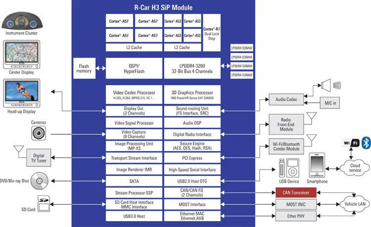
R-Car H3 is a 64-bit nona-core ARM SoC designed by Renesas for the automotive industry and introduced in 2016. The H3 incorporates four Cortex-A57 cores, four Cortex-A53 cores, and a dual-core lock-step Cortex-R7 for real-time processing. This chip supports up to quad-channel LPDDR4-3200 memory. This chip incorporates the Imagination's PowerVR GX6650 GPU.
Samples for the H3 were available starting December 2015 with Renesas expecting mass production to begin in March 2018 and reach a volume of 100,000 units per month in March 2019.
Contents
Cache[edit]
- Main articles: Cortex-A53 § Cache and Cortex-A57 § Cache
Cortex-A57 Cluster:
|
Cache Organization
Cache is a hardware component containing a relatively small and extremely fast memory designed to speed up the performance of a CPU by preparing ahead of time the data it needs to read from a relatively slower medium such as main memory. The organization and amount of cache can have a large impact on the performance, power consumption, die size, and consequently cost of the IC. Cache is specified by its size, number of sets, associativity, block size, sub-block size, and fetch and write-back policies. Note: All units are in kibibytes and mebibytes. |
|||||||||||||||||||||||||
|
|||||||||||||||||||||||||
Cortex-A53 Cluster:
|
Cache Organization
Cache is a hardware component containing a relatively small and extremely fast memory designed to speed up the performance of a CPU by preparing ahead of time the data it needs to read from a relatively slower medium such as main memory. The organization and amount of cache can have a large impact on the performance, power consumption, die size, and consequently cost of the IC. Cache is specified by its size, number of sets, associativity, block size, sub-block size, and fetch and write-back policies. Note: All units are in kibibytes and mebibytes. |
|||||||||||||||||||||||||
|
|||||||||||||||||||||||||
Memory controller[edit]
|
Integrated Memory Controller
|
||||||||||||||
|
||||||||||||||
Expansions[edit]
- PCI Express2.0 (1 lane) x 2 ch
- USB 3.0 Host interface (DRD) × 1 ports (wPHY)
- USB 2.0 Host/Function/OTG interface × 2 ports (wPHY)
- SD Host interface × 4 ch (SDR104)
- Multimedia card interface × 2 ch
- Serial ATA interface × 1 ch
- Media local bus (MLB) Interface × 1 ch (3 pin interface)
- Controller Area Network (CAN-FD support) Interface × 2ch
- Ethernet AVB 1.0-compatible MAC built in Interface: RGMII / Ethernet AVB (802.1BA)
- SYS-DMAC x 48 ch, Realtime-DMAC x 16 ch,
- Audio-DMAC x 32 ch, Audio(peripheral)-DMAC x 29 ch
- 32bit timer x 26 ch
- PWM timer × 7 ch
- I2C bus interface × 7 ch
- Serial communication interface (SCIF) × 11 ch
- Quad serial peripheral interface (QSPI) x 2 ch (for boot, HyperFlash support)
- Clock-synchronized serial interface (MSIOF) × 4 ch (SPI/IIS)
- Ethernet controller (IEEE802.3u, RMII, without PHY)
- Digital radio interface (DRIF) × 4 ch
Graphics[edit]
|
Integrated Graphics Information
|
||||||
|
||||||
Features[edit]
[Edit/Modify Supported Features]
|
Supported ARM Extensions & Processor Features
|
||||||
|
||||||
Block Diagram[edit]
Die[edit]
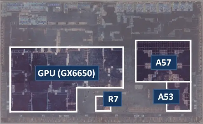
- 16 nm process, CMOS FinFET
- 12.94 mm × 8.61 mm
- 111.36 mm² die size
- Quad-core Cortex-A53
- ~3.27 mm² cluster
- ~0.60 mm² core
- ~0.7`mm² L2 cache
- Quad-core Cortex-A57
- ~10.21 mm² cluster
- ~1.66 mm² core
- ~3.28 mm² L2 cache
- Cortex-R7 (dual-core lock-step)
- ~1.04 mm² cluster
- GX6650 GPU
- ~28.12 mm²
Bibliography[edit]
- Takahashi, Chikafumi, et al. "4.5 A 16nm FinFET heterogeneous nona-core SoC complying with ISO26262 ASIL-B: Achieving 10− 7 random hardware failures per hour reliability." Solid-State Circuits Conference (ISSCC), 2016 IEEE International. IEEE, 2016.
- Shibahara, Shinichi, et al. "A 16 nm FinFET Heterogeneous Nona-Core SoC Supporting ISO26262 ASIL B Standard." IEEE Journal of Solid-State Circuits 52.1 (2017): 77-88.
Categories:
- all microprocessor models
- microprocessor models by renesas
- microprocessor models by renesas based on cortex-a53
- microprocessor models by renesas based on cortex-a57
- microprocessor models by renesas based on cortex-r7
- microprocessor models by arm holdings
- microprocessor models by arm holdings based on cortex-a53
- microprocessor models by arm holdings based on cortex-a57
- microprocessor models by arm holdings based on cortex-r7
- microprocessor models by tsmc
Facts about "R-Car H3 - Renesas"
| has ecc memory support | false + |
| integrated gpu | PowerVR GX6650 + |
| integrated gpu designer | Imagination Technologies + |
| l1$ size | 640 KiB (655,360 B, 0.625 MiB) + |
| l1d$ size | 288 KiB (294,912 B, 0.281 MiB) + |
| l1i$ size | 352 KiB (360,448 B, 0.344 MiB) + |
| l2$ size | 2.5 MiB (2,560 KiB, 2,621,440 B, 0.00244 GiB) + |
| max memory bandwidth | 47.68 GiB/s (48,824.32 MiB/s, 51.196 GB/s, 51,196.01 MB/s, 0.0466 TiB/s, 0.0512 TB/s) + |
| max memory channels | 4 + |
| supported memory type | LPDDR4-3200 + |

