From WikiChip
Difference between revisions of "intel/microarchitectures/p6"
| (10 intermediate revisions by 5 users not shown) | |||
| Line 9: | Line 9: | ||
| process = 350 nm | | process = 350 nm | ||
| process 2 = 250 nm | | process 2 = 250 nm | ||
| + | |isa=x86-32 | ||
| succession = Yes | | succession = Yes | ||
| Line 18: | Line 19: | ||
| successor 2 link = intel/microarchitectures/pentium_m | | successor 2 link = intel/microarchitectures/pentium_m | ||
}} | }} | ||
| − | '''P6''' was the [[microarchitecture]] for [[Intel]]'s for desktops and servers as a successor to {{\\|P5}}. Introduced in 1995 and continued until 2000, P6 was fabricated using [[350 nm]] and [[250 nm]] processes. P6 was | + | [[File:pentium pro processor with 1m l2 cache.jpg|right|thumb|{{intel|Pentium Pro}} processor with 1M of [[L2 cache]].]] |
| + | '''P6''' was the [[microarchitecture]] for [[Intel]]'s for desktops and servers as a successor to {{\\|P5}}. Introduced in 1995 and continued until 2000, P6 was fabricated using [[350 nm]] and [[250 nm]] processes. P6 was made obsolete by {{\\|NetBurst}} in late 2000. | ||
| + | |||
| + | == Codenames == | ||
| + | {{empty section}} | ||
== Process Technology == | == Process Technology == | ||
| − | P6 was manufactured on [[0.35 µm process]] initially and | + | P6 was manufactured on the [[0.35 µm process]] initially and later enjoyed a process shrink down to [[0.25 µm]], allowing for considerably lower voltage and higher clock speed at a smaller silicon die area. The shrink introduced a 5th metal layer which further reduced RC delay and die area. Intel claimed the channel area was reduced by 50% with the introduction of the 5th layer. The 5th layer also enabled Intel to support C4 packaging. |
{| class="wikitable" | {| class="wikitable" | ||
| Line 31: | Line 36: | ||
| Interconnect Pitch || 880 nm || 640 nm || 0.73x | | Interconnect Pitch || 880 nm || 640 nm || 0.73x | ||
|} | |} | ||
| + | |||
| + | == Compiler support == | ||
| + | {{empty section}} | ||
| + | |||
| + | == Architecture == | ||
| + | {{empty section}} | ||
== Die Shot == | == Die Shot == | ||
| + | [[File:p6 tualatin die slide.png|thumb|right|200px|Tualatin]] | ||
| + | === {{intel|Klamath|l=core}} === | ||
* [[280 nm process]] [[CMOS]] | * [[280 nm process]] [[CMOS]] | ||
* 4 metal layers | * 4 metal layers | ||
| Line 40: | Line 53: | ||
* 540-pin BGA (Ball Grid Array) | * 540-pin BGA (Ball Grid Array) | ||
[[File:intel p6 die shot.png]] | [[File:intel p6 die shot.png]] | ||
| + | |||
| + | === Pentium Pro === | ||
| + | * [[0.35 µm process]] | ||
| + | * 5,500,000 transistors | ||
| + | [[File:pentium pro die shot.png|700px]] | ||
== References == | == References == | ||
| Line 45: | Line 63: | ||
* Brand, Adam, et al. "Intel’s 0.25 micron, 2.0 volts logic process technology." Intel Technology Journal Q 3 (1998): 1998. | * Brand, Adam, et al. "Intel’s 0.25 micron, 2.0 volts logic process technology." Intel Technology Journal Q 3 (1998): 1998. | ||
* Integrated Circuit Engineering (ICE) Corporation. "Construction Analysis Intel 266MHz 32-Bit Pentium II (Klamath) Processor"; Shared Construction Analysis (SCA) 9706-542. | * Integrated Circuit Engineering (ICE) Corporation. "Construction Analysis Intel 266MHz 32-Bit Pentium II (Klamath) Processor"; Shared Construction Analysis (SCA) 9706-542. | ||
| + | |||
| + | == Documents == | ||
| + | * [[:File:24281603.pdf|Intel Architecture Optimization Manual]], Document 242816-003; 1997 | ||
Latest revision as of 20:34, 22 February 2020
| Edit Values | |
| P6 µarch | |
| General Info | |
| Arch Type | CPU |
| Designer | Intel |
| Manufacturer | Intel |
| Introduction | October, 1995 |
| Phase-out | December, 2000 |
| Process | 350 nm, 250 nm |
| Instructions | |
| ISA | x86-32 |
| Succession | |
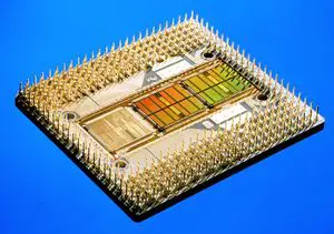
P6 was the microarchitecture for Intel's for desktops and servers as a successor to P5. Introduced in 1995 and continued until 2000, P6 was fabricated using 350 nm and 250 nm processes. P6 was made obsolete by NetBurst in late 2000.
Contents
Codenames[edit]
| This section is empty; you can help add the missing info by editing this page. |
Process Technology[edit]
P6 was manufactured on the 0.35 µm process initially and later enjoyed a process shrink down to 0.25 µm, allowing for considerably lower voltage and higher clock speed at a smaller silicon die area. The shrink introduced a 5th metal layer which further reduced RC delay and die area. Intel claimed the channel area was reduced by 50% with the introduction of the 5th layer. The 5th layer also enabled Intel to support C4 packaging.
| 0.35 µm | 0.25 µm | Δ | |
|---|---|---|---|
| Contacted Gate Pitch | 550 nm | 500 nm | 0.91x |
| Interconnect Pitch | 880 nm | 640 nm | 0.73x |
Compiler support[edit]
| This section is empty; you can help add the missing info by editing this page. |
Architecture[edit]
| This section is empty; you can help add the missing info by editing this page. |
Die Shot[edit]
Klamath[edit]
- 280 nm process CMOS
- 4 metal layers
- 7,500,000 transistors
- 13.3 mm x 14.6 mm
- 194.8 mm² die size
- 540-pin BGA (Ball Grid Array)
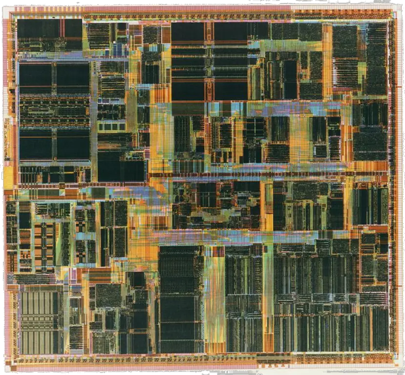
Pentium Pro[edit]
- 0.35 µm process
- 5,500,000 transistors
References[edit]
- Schutz, J., and R. Wallace. "A 450 MHz IA32 P6 family microprocessor." Solid-State Circuits Conference, 1998. Digest of Technical Papers. 1998 IEEE International. IEEE, 1998.
- Brand, Adam, et al. "Intel’s 0.25 micron, 2.0 volts logic process technology." Intel Technology Journal Q 3 (1998): 1998.
- Integrated Circuit Engineering (ICE) Corporation. "Construction Analysis Intel 266MHz 32-Bit Pentium II (Klamath) Processor"; Shared Construction Analysis (SCA) 9706-542.
Documents[edit]
- Intel Architecture Optimization Manual, Document 242816-003; 1997
Facts about "P6 - Microarchitectures - Intel"
| codename | P6 + |
| designer | Intel + |
| first launched | October 1995 + |
| full page name | intel/microarchitectures/p6 + |
| instance of | microarchitecture + |
| manufacturer | Intel + |
| microarchitecture type | CPU + |
| name | P6 + |
| phase-out | December 2000 + |
| process | 350 nm (0.35 μm, 3.5e-4 mm) + and 250 nm (0.25 μm, 2.5e-4 mm) + |


