(Foveros) |
|||
| Line 1: | Line 1: | ||
{{intel title|Foveros}}{{packaging}} | {{intel title|Foveros}}{{packaging}} | ||
| − | '''Foveros''' is a proprietary high-performance [[three-dimensional integrated circuit]] (3D IC) packaging technology designed by [[Intel]]. | + | '''Foveros''' is a proprietary high-performance [[three-dimensional integrated circuit]] (3D IC) packaging face-to-face-based technology designed by [[Intel]]. |
| + | |||
| + | == Overview == | ||
| + | [[File:intel foveros slide 1.png|left|thumb|Foveros]] | ||
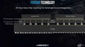
| + | First introduced in 2019, Foveros is an advanced 3D face-to-face die stacking packaging process technology. The technology is designed to incorporate two or more [[chiplets]] assembled together. It comprises a base logic die on top of which sit additional active components such as another logic die, memory, FPGA, or even analog/RF. | ||
| + | |||
| + | |||
| + | :[[File:intel-foveros.svg|600px]] | ||
| + | |||
| + | |||
| + | The key feature of Foveros is the face-to-face (F2F) chip-on-chip bonding through extremely fin-pitched, 36-micron, microbumps (mostly likely copper pillars). F2F flow is somewhat fairly straightforward. Bumping is done to the base and top dies followed by backgrinding and then singulation. They likely use TCB-NCP for the final assembly, but this is pure speculation. The main benefits of F2F are the interconnect density scaling and lower wire parasitics which is important of high-performance applications like those used by Intel. | ||
| + | |||
| + | == Motivation == | ||
| + | The move to [[chiplets]] meant new challenges. One of those challenges involves communication between the dies. Moving a bit on-die is an order of magnitude lower than moving a bit off-die. Likewise, by leaving the silicon, wires become thicker and occupy more area, making bandwidth and footprint a challenge. Forveros is Intel's solution to this challenge. By moving the die on top of a second die and connecting them in a face-to-face manner means the bumps can be much smaller which means lower wire parasitics and higher density. Additionally, through clever designs, it's possible to significantly improve the latency and/or bandwidth of certain components by stacking the storage on top of the active components. | ||
Revision as of 21:26, 12 May 2019
| Packaging | |
 | |
| Technologies | |
| Concepts | |
| Single-Row | |
| Dual-Row | |
| Quad-Row | |
| Grid Array | |
| 2.5D IC | |
| 3D IC | |
Foveros is a proprietary high-performance three-dimensional integrated circuit (3D IC) packaging face-to-face-based technology designed by Intel.
Overview
First introduced in 2019, Foveros is an advanced 3D face-to-face die stacking packaging process technology. The technology is designed to incorporate two or more chiplets assembled together. It comprises a base logic die on top of which sit additional active components such as another logic die, memory, FPGA, or even analog/RF.
The key feature of Foveros is the face-to-face (F2F) chip-on-chip bonding through extremely fin-pitched, 36-micron, microbumps (mostly likely copper pillars). F2F flow is somewhat fairly straightforward. Bumping is done to the base and top dies followed by backgrinding and then singulation. They likely use TCB-NCP for the final assembly, but this is pure speculation. The main benefits of F2F are the interconnect density scaling and lower wire parasitics which is important of high-performance applications like those used by Intel.
Motivation
The move to chiplets meant new challenges. One of those challenges involves communication between the dies. Moving a bit on-die is an order of magnitude lower than moving a bit off-die. Likewise, by leaving the silicon, wires become thicker and occupy more area, making bandwidth and footprint a challenge. Forveros is Intel's solution to this challenge. By moving the die on top of a second die and connecting them in a face-to-face manner means the bumps can be much smaller which means lower wire parasitics and higher density. Additionally, through clever designs, it's possible to significantly improve the latency and/or bandwidth of certain components by stacking the storage on top of the active components.

