Semiconductor & Computer Engineering
From WikiChip
Difference between revisions of "intel/core m/m7-6y75"
| (2 intermediate revisions by one other user not shown) | |||
| Line 1: | Line 1: | ||
{{intel title|Core m7-6Y75}} | {{intel title|Core m7-6Y75}} | ||
| − | {{ | + | {{chip |
|name=Core m7-6Y75 | |name=Core m7-6Y75 | ||
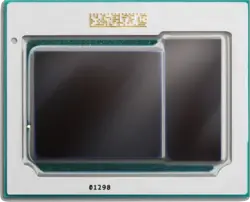
|image=skylake y (front).png | |image=skylake y (front).png | ||
| Line 19: | Line 19: | ||
|turbo frequency1=3,100 MHz | |turbo frequency1=3,100 MHz | ||
|turbo frequency2=2,900 MHz | |turbo frequency2=2,900 MHz | ||
| + | |turbo frequency=Yes | ||
|bus type=DMI 3.0 | |bus type=DMI 3.0 | ||
|clock multiplier=12 | |clock multiplier=12 | ||
| Line 50: | Line 51: | ||
|tjunc min=5 °C | |tjunc min=5 °C | ||
|tjunc max=100 °C | |tjunc max=100 °C | ||
| − | |package | + | |package name 1=intel,fcbga_1515 |
| − | |||
}} | }} | ||
'''Core M7-6Y75''' is an ultra-low power {{arch|64}} [[dual-core]] [[x86]] microprocessor introduced by [[Intel]] in late 2015. This MPU operates at 1.2 GHz with a max turbo frequency of 3.1 GHz. This chip, which is manufactured on a [[14 nm process]], is based on the {{intel|Skylake}} microarchitecture. The Core M7-6Y75 incorporates Intel's {{intel|HD Graphics 515}} Gen9 GPU clocked at 300 MHz with turbo frequency of 1 GHz. | '''Core M7-6Y75''' is an ultra-low power {{arch|64}} [[dual-core]] [[x86]] microprocessor introduced by [[Intel]] in late 2015. This MPU operates at 1.2 GHz with a max turbo frequency of 3.1 GHz. This chip, which is manufactured on a [[14 nm process]], is based on the {{intel|Skylake}} microarchitecture. The Core M7-6Y75 incorporates Intel's {{intel|HD Graphics 515}} Gen9 GPU clocked at 300 MHz with turbo frequency of 1 GHz. | ||
| Line 165: | Line 165: | ||
|avx=Yes | |avx=Yes | ||
|avx2=Yes | |avx2=Yes | ||
| − | + | ||
|abm=Yes | |abm=Yes | ||
|tbm=No | |tbm=No | ||
Latest revision as of 16:58, 28 August 2018
| Edit Values | |
| Core m7-6Y75 | |
 | |
| General Info | |
| Designer | Intel |
| Manufacturer | Intel |
| Model Number | m7-6Y75 |
| Part Number | HE8066201922875 |
| S-Spec | SR2EH |
| Market | Mobile |
| Introduction | September 1, 2015 (announced) September 27, 2015 (launched) |
| Release Price | $393 |
| Shop | Amazon |
| General Specs | |
| Family | Core m7 |
| Series | m-6Y |
| Locked | Yes |
| Frequency | 1200 MHz |
| Turbo Frequency | Yes |
| Turbo Frequency | 3,100 MHz (1 core), 2,900 MHz (2 cores) |
| Bus type | DMI 3.0 |
| Clock multiplier | 12 |
| Microarchitecture | |
| ISA | x86-64 (x86) |
| Microarchitecture | Skylake |
| Platform | Skylake |
| Core Name | Skylake Y |
| Core Family | 6 |
| Core Model | 78 |
| Core Stepping | D1 |
| Process | 14 nm |
| Transistors | 1,750,000,000 |
| Technology | CMOS |
| Die | 98.57 mm² 10.3 mm × 9.57 mm |
| MCP | Yes (2 dies) |
| Word Size | 64 bit |
| Cores | 2 |
| Threads | 4 |
| Max Memory | 16 GiB |
| Multiprocessing | |
| Max SMP | 1-Way (Uniprocessor) |
| Electrical | |
| SDP | 3 W |
| TDP | 4.5 W |
| cTDP down | 3.5 W |
| cTDP down frequency | 600 MHz |
| cTDP up | 7 W |
| cTDP up frequency | 1500 MHz |
| Tjunction | 5 °C – 100 °C |
| Packaging | |
| Package | FCBGA-1515 (BGA) |
| Dimension | 20 mm × 16.5 mm × 0.5 mm |
| Pitch | 0.4 mm |
| Contacts | 1515 |
Core M7-6Y75 is an ultra-low power 64-bit dual-core x86 microprocessor introduced by Intel in late 2015. This MPU operates at 1.2 GHz with a max turbo frequency of 3.1 GHz. This chip, which is manufactured on a 14 nm process, is based on the Skylake microarchitecture. The Core M7-6Y75 incorporates Intel's HD Graphics 515 Gen9 GPU clocked at 300 MHz with turbo frequency of 1 GHz.
Cache[edit]
- Main article: Skylake § Cache
|
Cache Organization
Cache is a hardware component containing a relatively small and extremely fast memory designed to speed up the performance of a CPU by preparing ahead of time the data it needs to read from a relatively slower medium such as main memory. The organization and amount of cache can have a large impact on the performance, power consumption, die size, and consequently cost of the IC. Cache is specified by its size, number of sets, associativity, block size, sub-block size, and fetch and write-back policies. Note: All units are in kibibytes and mebibytes. |
|||||||||||||||||||||||||||||||||||||
|
|||||||||||||||||||||||||||||||||||||
Memory controller[edit]
|
Integrated Memory Controller
|
||||||||||||||
|
||||||||||||||
Expansions[edit]
|
Expansion Options
|
||||||||
|
||||||||
Graphics[edit]
|
Integrated Graphics Information
|
||||||||||||||||||||||||||||||||||||||||||||||||||||||||||||||||||||
|
||||||||||||||||||||||||||||||||||||||||||||||||||||||||||||||||||||
| [Edit] Skylake (Gen9) Hardware Accelerated Video Capabilities | |||||||
|---|---|---|---|---|---|---|---|
| Codec | Encode | Decode | |||||
| Profiles | Levels | Max Resolution | Profiles | Levels | Max Resolution | ||
| MPEG-2 (H.262) | Main | High | 1080p (FHD) | Main | Main, High | 1080p (FHD) | |
| MPEG-4 AVC (H.264) | High, Main | 5.1 | 2160p (4K) | Main, High, SHP, MHP | 5.1 | 2160p (4K) | |
| JPEG/MJPEG | Baseline | - | 16k x 16k | Baseline | Unified | 16k x 16k | |
| HEVC (H.265) | Main | 5.1 | 2160p (4K) | Main, Main 10 | 5.1 | 2160p (4K) | |
| VC-1 | ✘ | Advanced, Main, Simple | 3, High | 3840x3840 | |||
| VP8 | Unified | Unified | - | 0 | Unified | 1080p | |
| VP9 | ✘ | 0 | Unified | 2160p (4K) | |||
Features[edit]
[Edit/Modify Supported Features]
|
Supported x86 Extensions & Processor Features
|
||||||||||||||||||||||||||||||||||||||||||||||||||||||||||||||||||||||||||||||||||||||
|
||||||||||||||||||||||||||||||||||||||||||||||||||||||||||||||||||||||||||||||||||||||
Drivers[edit]
Facts about "Core m7-6Y75 - Intel"