(nvswitch) |
|||
| (6 intermediate revisions by one other user not shown) | |||
| Line 1: | Line 1: | ||
{{nvidia title|NVSwitch}} | {{nvidia title|NVSwitch}} | ||
| − | {{chip}} | + | {{chip |
| + | |chip type=integrated circuit | ||
| + | |name=NVSwitch | ||
| + | |no image=Yes | ||
| + | |designer=Nvidia | ||
| + | |manufacturer=TSMC | ||
| + | |market=Server | ||
| + | |market 2=Workstation | ||
| + | |first announced=March 27, 2018 | ||
| + | |first launched=March 27, 2018 | ||
| + | |transistors=2,000,0000,000 | ||
| + | |technology=CMOS | ||
| + | |power=100 W | ||
| + | }} | ||
'''NVSwitch''' is an 18-port {{nvidia|NVLink}} switch. Fabricated on [[TSMC]]'s [[12 nm process]] for a total of 2 billion transistors, the switch has a total bandwidth of 900 GB/s. The NVSwitch is currently only utilized in Nvidia's own {{nvidia|DGX-2}} AI computer. | '''NVSwitch''' is an 18-port {{nvidia|NVLink}} switch. Fabricated on [[TSMC]]'s [[12 nm process]] for a total of 2 billion transistors, the switch has a total bandwidth of 900 GB/s. The NVSwitch is currently only utilized in Nvidia's own {{nvidia|DGX-2}} AI computer. | ||
| + | |||
| + | == Overview == | ||
| + | The NVSwitch was introduced with the launch of Nvidia's {{nvidia|DGX-2}} computer. The NVSwitch is a 2 billion transistor, 18-port, {{nvidia|NVLink}} switch. With each port operating at 50 GB/s, the switch has a total bandwidth of 900 GB/s. The switch allows up to any nine devices to be routed to any of the other nine devices. In addition to the NVLink ports, the switch has addition I/O for control and management including x4 [[PCIe]] Gen 2 management port, [[I²C]], and [[GPIO]]. | ||
| + | |||
| + | |||
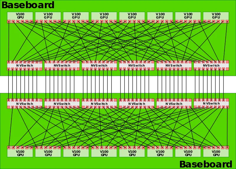
| + | The DGX-2 uses 6 NVLinks per baseboard to create a fully-connected network of GPUs. | ||
| + | |||
| + | |||
| + | :[[File:dgx2 nvswitch baseboard diagram.svg|800px]] | ||
| + | |||
| + | |||
| + | The DGX-2 has two baseboards to fully connect all 16 {{nvidia|V100}} GPUs to each other. Each switch does have 2 ports unused. It's possible those ports will be used in configurations involving the {{ibm|POWER9}} microprocessors which have native support for NVLink 2.0. | ||
| + | |||
| + | |||
| + | :[[File:dgx2 nvswitch baseboard diagram with two boards connected.svg|800px]] | ||
| + | |||
| + | == Die == | ||
| + | * TSMC's [[12 nm process|12nm FFN (Nvidia) process]] | ||
| + | * 2,000,000,000 transistors | ||
| + | * 20mm x 20mm (4 cm²) BGA package | ||
| + | ** 1,940 pins | ||
| + | ** 576 NVLink signals | ||
| + | |||
| + | |||
| + | :[[File:nvidia nvswitch die shot.png|1200px]] | ||
| + | |||
| + | |||
| + | :[[File:nvidia nvswitch die shot (annotated).png|1200px]] | ||
| + | |||
| + | == See also == | ||
| + | * {{nvidia|NVLink}} | ||
| + | |||
| + | == Reference == | ||
| + | * Nvidia, GTC 2018, March 2018 | ||
Latest revision as of 03:18, 26 August 2018
| Edit Values | |
| NVSwitch | |
| General Info | |
| Designer | Nvidia |
| Manufacturer | TSMC |
| Market | Server, Workstation |
| Introduction | March 27, 2018 (announced) March 27, 2018 (launched) |
| Microarchitecture | |
| Transistors | 2,000,0000,000 |
| Technology | CMOS |
| Electrical | |
| Power dissipation | 100 W |
NVSwitch is an 18-port NVLink switch. Fabricated on TSMC's 12 nm process for a total of 2 billion transistors, the switch has a total bandwidth of 900 GB/s. The NVSwitch is currently only utilized in Nvidia's own DGX-2 AI computer.
Contents
Overview[edit]
The NVSwitch was introduced with the launch of Nvidia's DGX-2 computer. The NVSwitch is a 2 billion transistor, 18-port, NVLink switch. With each port operating at 50 GB/s, the switch has a total bandwidth of 900 GB/s. The switch allows up to any nine devices to be routed to any of the other nine devices. In addition to the NVLink ports, the switch has addition I/O for control and management including x4 PCIe Gen 2 management port, I²C, and GPIO.
The DGX-2 uses 6 NVLinks per baseboard to create a fully-connected network of GPUs.
The DGX-2 has two baseboards to fully connect all 16 V100 GPUs to each other. Each switch does have 2 ports unused. It's possible those ports will be used in configurations involving the POWER9 microprocessors which have native support for NVLink 2.0.
Die[edit]
- TSMC's 12nm FFN (Nvidia) process
- 2,000,000,000 transistors
- 20mm x 20mm (4 cm²) BGA package
- 1,940 pins
- 576 NVLink signals
See also[edit]
Reference[edit]
- Nvidia, GTC 2018, March 2018
| designer | Nvidia + |
| first announced | March 27, 2018 + |
| first launched | March 27, 2018 + |
| full page name | nvidia/nvswitch + |
| instance of | integrated circuit + |
| ldate | March 27, 2018 + |
| manufacturer | TSMC + |
| market segment | Server + and Workstation + |
| name | NVSwitch + |
| power dissipation | 100 W (100,000 mW, 0.134 hp, 0.1 kW) + |
| technology | CMOS + |


