(→Die Shot) |
|||
| Line 95: | Line 95: | ||
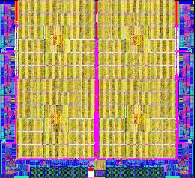
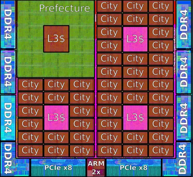
== Die Shot == | == Die Shot == | ||
| − | [[File:pezy sc die shot.jpg| | + | [[File:pezy sc die shot.jpg|650px]] |
| + | |||
| + | |||
| + | [[File:pezy-sc die shot (annotated).png|650px]] | ||
== Cache == | == Cache == | ||
Revision as of 21:28, 6 September 2016
Template:mpu PEZY-SC (PEZY Super Computer) is second generation many-core microprocessor developed by PEZY in 2014. PEZY-SC contains 2 ARM926 cores (ARMv5TEJ) along with 1024 simpler RISC cores. Operating at 733 MHz, the processor is said to have peach performance of 3.0 TFLOPS (single-precision) and 1.5 TFLOPS (double-precision). PEZY-SC was designed using 580 million gates and manufactured on TSMC's 28HPC+ (28 nm process). The PEZY-SC is used in a number of TOP500 & Green500 supercomputers as the world's most efficient supercomputers.
Contents
Overview
- See also: PEZY-1
The PEZY-SC (SC for "Super Computer") is PEZY's second generation microprocessors which builds upon the PEZY-1. The chip contains exactly twice as many cores and incorporates a large amount of cache including 8 MB of L3$.
In June of 2015, PEZY-SC-based supercomputers took all top 3 spots on the Green500 listing as the 3 most efficient supercomputers. PEZY-SC powers Shoubu (1,181,952 cores, ? kW, 605.624 TFlop/s Linpack Rmax), and Suiren Blue (262,656 cores, 40.86 kW, 247.752 TFlop/s Linpack Rmax), and Suiren (328,480 cores, 48.90 kW, 271.782 TFlop/s Linpack Rmax) supercomputers (ranked 1, 2, and 3 respectively).
Architecture
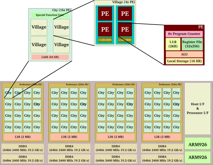
The PEZY-SC microprocessors is made of 4 blocks called "Prefectures". The Prefecture contains 2 MB of L3$ enclosed by 16 smaller blocks called "Cities". Each City is made of 64 KB of L2$, a number of special function units, and 4 smaller blocks called "Villages". A village is a block of 4 execution units. For ever 2 execution units there are 2 KB of L1d$.
Processor Element (PE)
The PE are the individual execution cores.
| This section requires expansion; you can help adding the missing info. |
Die Shot
Cache
PEZY-SC's cache is separate from the ARM926's cache which has an L1$ of 32KB (2x) and 64KB L2$ (shared).
| Cache Info [Edit Values] | ||
| L1I$ | 2 MB "MB" is not declared as a valid unit of measurement for this property. |
1024x2 KB (per processor element) |
| L1D$ | 1 MB "MB" is not declared as a valid unit of measurement for this property. |
512x2 KB (per 2 processor elements) |
| L2$ | 4 MB "MB" is not declared as a valid unit of measurement for this property. |
4x2 MB (per city) |
| L3$ | 8 MB "MB" is not declared as a valid unit of measurement for this property. |
4x2 MB (per prefecture) |
Memory controller
| Integrated Memory Controller | |
| Type | DDR4-1333 |
| Controllers | 1 |
| Channels | 8 |
| Bandwidth (single) | 10,600 MB/s |
| Bandwidth (dual) | 21,200 MB/s |
| Bandwidth (quad) | 42,400 MB/s |
| Bandwidth (octa) | 84,800 MB/s |


