From WikiChip
Difference between revisions of "mathstar/arrix"
(→MOA2400D Series) |
|||
| (6 intermediate revisions by the same user not shown) | |||
| Line 12: | Line 12: | ||
| first launched = November 29, 2006 | | first launched = November 29, 2006 | ||
| production start = 2006 | | production start = 2006 | ||
| − | | production end = | + | | production end = 2009 |
| arch = | | arch = | ||
| microarch = | | microarch = | ||
| Line 18: | Line 18: | ||
| proc = 130 nm | | proc = 130 nm | ||
| proc 2 = 90 nm | | proc 2 = 90 nm | ||
| − | |||
| − | |||
| tech = CMOS | | tech = CMOS | ||
| − | | clock min = | + | | clock min = 400 MHz |
| − | | clock max = 1, | + | | clock max = 1,000 MHz |
| package = FCBGA-896 | | package = FCBGA-896 | ||
| package 2 = | | package 2 = | ||
| Line 28: | Line 26: | ||
| socket = FCBGA-896 | | socket = FCBGA-896 | ||
| socket 2 = | | socket 2 = | ||
| − | | socket | + | | socket 3 = |
| succession = Yes | | succession = Yes | ||
| Line 36: | Line 34: | ||
| successor link = | | successor link = | ||
}} | }} | ||
| − | '''Arrix''' was a family of [[field-programmable object array]] designed by [[MathStar]] and introduced in late [[2006]]. | + | '''Arrix''' was a family of [[field-programmable object array]] designed by [[MathStar]] and introduced in late [[2006]]. MathStar continued manufacturing this until 2009. |
== Architecture == | == Architecture == | ||
| − | {{ | + | {{main|field-programmable object array}} |
| + | Arrix is a family of [[field-programmable object array]] (FPOA). The chips can operate, depending on model, from 400 MHz to 1 GHz. At the time their performance exceeded similar budget [[FPGA]]s. Arrix are a grid of 400 logic objects. Additionally the chips also feature: | ||
| + | |||
| + | * 2x Bi-directional 500MHz DDR 16-bit LVDS ports | ||
| + | * 96x GPIO (synchronously or asynchronously at up to 100 MHz) | ||
| + | * 12x banks of 500MHz internal SRAM memory banks | ||
| + | * 2x 266 MHz 36-bit DDR (72-bits per cycle) RLDRAM II controllers | ||
| + | |||
| + | The chips are arranged as a grid of 400 logic objects made up of: | ||
| + | |||
| + | * 256x [[arithmetic logic unit|ALU]] | ||
| + | ** 16 bit data, 5 bits control, 32 operations | ||
| + | ** {{arch|16}} add/sub/shift/rotate/AND/OR/XOR | ||
| + | ** circuitry for cascading status bits for making larger word | ||
| + | * 80x [[register file|RFs]] | ||
| + | ** 128 Byte, dualport RAM or FIFO | ||
| + | * 64x [[multiply accumulator|MAC]]x | ||
| + | ** 16x16 single clock cycle [[multiplier]] | ||
| + | ** 32 bit intermediate result, signed or unsigned | ||
| + | ** 40 bit [[accumulator]], 256 accumulations before [[overflow]] | ||
| + | * 12x Internal [[RAM]] banks | ||
| + | ** 768 x 76 bits | ||
| + | [[File:arrix chip layout.png|600px]] | ||
== Members == | == Members == | ||
| Line 46: | Line 66: | ||
{| class="wikitable sortable" | {| class="wikitable sortable" | ||
|- | |- | ||
| − | ! Model !! Frequency !! | + | ! Model !! Frequency !! Objects !! Package !! Temp Range |
|- | |- | ||
| {{\|MOA2400D-10}} || 1,000 MHz || 400 || FCBGA-896 || Commercial | | {{\|MOA2400D-10}} || 1,000 MHz || 400 || FCBGA-896 || Commercial | ||
| Line 68: | Line 88: | ||
| {{\|MOA2400D-04R}} || 400 MHz || 400 || FCBGA-896 RoHS || Commercial | | {{\|MOA2400D-04R}} || 400 MHz || 400 || FCBGA-896 RoHS || Commercial | ||
|} | |} | ||
| + | |||
| + | == Documents == | ||
| + | |||
| + | === Product Brief === | ||
| + | * [[:File:Arrix Family Product Brief (April 2007).pdf|Arrix Family Product Brief]], April 2007 | ||
| + | * [[:File:Arrix Family Product Brief (August 2006).pdf|Arrix Family Product Brief]], August 2006 | ||
| + | * [[:File:MOA1400D Product Brief (February 2006).pdf|MOA1400D Product Brief]], February 2006 | ||
| + | |||
| + | === IP Cores === | ||
| + | * [[:File:Color Space Conversion (RGB to YCRCB) for Arrix FPOA.pdf|Color Space Conversion (RGB to YCRCB) for Arrix FPOA]] | ||
| + | * [[:File:Flat Field Correction for Arrix FPOA.pdf|Flat Field Correction for Arrix FPOA]] | ||
| + | * [[:File:JPEG 2000 Encoder for Arrix FPOA.pdf|JPEG 2000 Encoder for Arrix FPOA]] | ||
| + | * [[:File:MPEG2 Multi-channel Decoder for FPOA.pdf|MPEG2 Multi-channel Decoder for FPOA]] | ||
| + | |||
| + | === Software === | ||
| + | * [[:File:Silicon Objects Software Development Environment.pdf|Silicon Objects Software Development Environment]] | ||
| + | |||
| + | === Manuals === | ||
| + | * [[:File:Arrix Family - FPOA Architecture Guide.pdf|Arrix Family - FPOA Architecture Guide]] | ||
| + | |||
| + | === Other === | ||
| + | * [[:File:Radiation HardenedField Programmable Object Array (FPOA) for Space Processing.pdf|Radiation HardenedField Programmable Object Array (FPOA) for Space Processing]] | ||
| + | |||
| + | == See also == | ||
| + | * [[field-programmable object array]] | ||
| + | * Ambric's {{ambric|Am2000}} | ||
Latest revision as of 23:37, 27 June 2016
| Arrix | |

| |
| Developer | MathStar |
| Manufacturer | TSMC |
| Type | Programmable logic device |
| Introduction | September 25, 2006 (announced) November 29, 2006 (launch) |
| Production | 2006-2009 |
| Word size | 16 bit 2 octets
4 nibbles |
| Process | 130 nm 0.13 μm , 90 nm1.3e-4 mm 0.09 μm
9.0e-5 mm |
| Technology | CMOS |
| Clock | 400 MHz-1,000 MHz |
| Package | FCBGA-896 |
| Socket | FCBGA-896 |
| Succession | |
| ← | |
| Builder | |
Arrix was a family of field-programmable object array designed by MathStar and introduced in late 2006. MathStar continued manufacturing this until 2009.
Contents
Architecture[edit]
- Main article: field-programmable object array
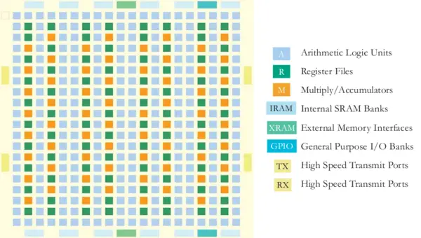
Arrix is a family of field-programmable object array (FPOA). The chips can operate, depending on model, from 400 MHz to 1 GHz. At the time their performance exceeded similar budget FPGAs. Arrix are a grid of 400 logic objects. Additionally the chips also feature:
- 2x Bi-directional 500MHz DDR 16-bit LVDS ports
- 96x GPIO (synchronously or asynchronously at up to 100 MHz)
- 12x banks of 500MHz internal SRAM memory banks
- 2x 266 MHz 36-bit DDR (72-bits per cycle) RLDRAM II controllers
The chips are arranged as a grid of 400 logic objects made up of:
- 256x ALU
- 16 bit data, 5 bits control, 32 operations
- 16-bit add/sub/shift/rotate/AND/OR/XOR
- circuitry for cascading status bits for making larger word
- 80x RFs
- 128 Byte, dualport RAM or FIFO
- 64x MACx
- 16x16 single clock cycle multiplier
- 32 bit intermediate result, signed or unsigned
- 40 bit accumulator, 256 accumulations before overflow
- 12x Internal RAM banks
- 768 x 76 bits
Members[edit]
MOA2400D Series[edit]
| Model | Frequency | Objects | Package | Temp Range |
|---|---|---|---|---|
| MOA2400D-10 | 1,000 MHz | 400 | FCBGA-896 | Commercial |
| MOA2400D-10R | 1,000 MHz | 400 | FCBGA-896 RoHS | Commercial |
| MOA2400D-09 | 900 MHz | 400 | FCBGA-896 | Industrial |
| MOA2400D-09R | 900 MHz | 400 | FCBGA-896 RoHS | Industrial |
| MOA2400D-08 | 800 MHz | 400 | FCBGA-896 | Industrial |
| MOA2400D-08R | 800 MHz | 400 | FCBGA-896 RoHS | Industrial |
| MOA2400D-06 | 600 MHz | 400 | FCBGA-896 | Industrial |
| MOA2400D-06R | 600 MHz | 400 | FCBGA-896 RoHS | Industrial |
| MOA2400D-04 | 400 MHz | 400 | FCBGA-896 | Commercial |
| MOA2400D-04R | 400 MHz | 400 | FCBGA-896 RoHS | Commercial |
Documents[edit]
Product Brief[edit]
- Arrix Family Product Brief, April 2007
- Arrix Family Product Brief, August 2006
- MOA1400D Product Brief, February 2006
IP Cores[edit]
- Color Space Conversion (RGB to YCRCB) for Arrix FPOA
- Flat Field Correction for Arrix FPOA
- JPEG 2000 Encoder for Arrix FPOA
- MPEG2 Multi-channel Decoder for FPOA
Software[edit]
Manuals[edit]
Other[edit]
See also[edit]
- field-programmable object array
- Ambric's Am2000
Facts about "Arrix - MathStar"
| designer | MathStar + |
| first announced | September 25, 2006 + |
| first launched | November 29, 2006 + |
| full page name | mathstar/arrix + |
| instance of | integrated circuit family + |
| main designer | MathStar + |
| manufacturer | TSMC + |
| name | Arrix + |
| package | FCBGA-896 + |
| process | 130 nm (0.13 μm, 1.3e-4 mm) + and 90 nm (0.09 μm, 9.0e-5 mm) + |
| socket | FCBGA-896 + |
| technology | CMOS + |
| word size | 16 bit (2 octets, 4 nibbles) + |
