(→iCAP: Fixed some article links) |
(→Versions) |
||
| (4 intermediate revisions by 4 users not shown) | |||
| Line 3: | Line 3: | ||
== Overview == | == Overview == | ||
| − | CoWoS is a [[2.5D]] wafer-level [[chiplet|multi-chip]] [[packaging technology]] that incorporates multiple [[dies]] side-by-side on a [[silicon interposer]] in order to achieve better interconnect density and performance. Individual chips are bonded through [[micro-bumps]] on a silicon interposer forming a chip-on-wafer (CoW). The CoW is then subsequently thinned such that the [[TSV]] perforations are exposed. This is followed [[C4 bumps]] formation and [[singulation]]. A CoWoS package is completed through bonding to a package substrate. | + | CoWoS is a [[2.5D]] wafer-level [[chiplet|multi-chip]] [[packaging technology]] that incorporates multiple [[dies]] side-by-side on a [[silicon interposer]] in order to achieve better interconnect density and performance. Individual chips are bonded through [[micro-bumps]] on a silicon interposer forming a chip-on-wafer (CoW). The CoW is then subsequently thinned such that the [[through-silicon_via|TSV]] perforations are exposed. This is followed [[C4 bumps]] formation and [[singulation]]. A CoWoS package is completed through bonding to a package substrate. |
| Line 25: | Line 25: | ||
| 2017 || 1.75 (~1500 mm²) || Logic+Logic/HBM2 || 900 GB/s | | 2017 || 1.75 (~1500 mm²) || Logic+Logic/HBM2 || 900 GB/s | ||
|- | |- | ||
| − | | 2019 || 1.85 (~1590 mm²) || Logic+Logic/HBM2 || 1 | + | | 2019 || 1.85 (~1590 mm²) || Logic+Logic/HBM2 || 1 TB/s |
|- | |- | ||
| − | | 2020 || 2x (~1700 mm²) || Logic+Logic/HBM2E/3 || 2.7 | + | | 2020 || 2x (~1700 mm²) || Logic+Logic/HBM2E/3 || 2.7 TB/s |
|- | |- | ||
| − | | | + | | 2022 || 3x (~2500 mm²) || Logic+Logic/HBM3 || Up to 8.6 Tb/s |
|} | |} | ||
| Line 43: | Line 43: | ||
{{clear}} | {{clear}} | ||
| − | === iCAP === | + | === Integrated Capacitor (iCAP) === |
{{see also|deep_trench_capacitor|l1=deep trench capacitor (DTC)}} | {{see also|deep_trench_capacitor|l1=deep trench capacitor (DTC)}} | ||
| − | TSMC | + | TSMC announced '''Integrated Capacitor''' ('''iCAP''') in 2019. iCAPs are CoWoS [[deep_trench_capacitor|deep trench capacitors]] with a standard cell of 40 [[µm]] by 40 µm. While TSMC was unwilling to disclose the depth of the trenches, the [[capacitance density]] it is able to achieve is up to 340 [[nF/mm²]]. This translates to close to 20x improvement in capacitance density over the HD-MiM. Since multiple iCAPs can be used on a single interposer, the total capacitance possible is over 68 μF per Si interposer. iCAPs are high-yielding and have reported leakage currents below 1 fA/μm², including at high temperatures. TSMC reported very good PDN improvements with iCAP. Compared to equivalent CoWoS-based design without iCAP, TSMC is reporting just 0.05x the impedance and 0.45x the voltage droop. |
| − | Since both [[TSVs]] and [[deep_trench_capacitor|DTCs]] co-exist on the same [[silicon wafer]], there are two ways to construct iCAPs. In the DTC-first approach, the deep trenches are formed prior to the TSV process which means special care must be taken to ensure the TSV thermal budget does not impact the DTCs. Alternatively, in a TSV-first flow, the TSV structures are formed first using the standard TSV process, but special care must be taken to mitigate TSV related issues such as the via protrusion phenomenon. Like HD-MiMs, a major benefit of DTC over package decaps is that they can be freely placed as close as possible to the desired circuit similar to on-chip decaps but with the added benefit that the deep trenches allow for much higher capacitance. Additionally, since this can be implemented across an entire 1700 mm2 interposer with all kinds of chips on top, the DTCs can be more finely designed to better address the PI of the chip above it. | + | Since both [[through-silicon_via|TSVs]] and [[deep_trench_capacitor|DTCs]] co-exist on the same [[silicon wafer]], there are two ways to construct iCAPs. In the DTC-first approach, the deep trenches are formed prior to the TSV process which means special care must be taken to ensure the TSV thermal budget does not impact the DTCs. Alternatively, in a TSV-first flow, the TSV structures are formed first using the standard TSV process, but special care must be taken to mitigate TSV related issues such as the via protrusion phenomenon. Like HD-MiMs, a major benefit of DTC over package decaps is that they can be freely placed as close as possible to the desired circuit similar to on-chip decaps but with the added benefit that the deep trenches allow for much higher capacitance. Additionally, since this can be implemented across an entire 1700 mm2 interposer with all kinds of chips on top, the DTCs can be more finely designed to better address the PI of the chip above it. |
<div> | <div> | ||
Latest revision as of 16:12, 15 May 2024
| Packaging | |
 | |
| Technologies | |
| Concepts | |
| Single-Row | |
| Dual-Row | |
| Quad-Row | |
| Grid Array | |
| 2.5D IC | |
| 3D IC | |
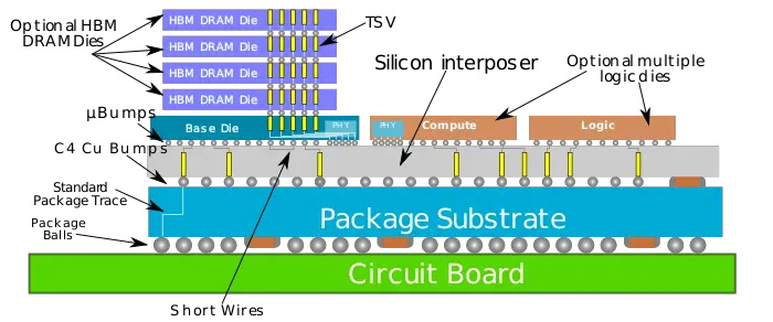
Chip-on-Wafer-on-Substrate (CoWoS) is a two-point-five dimensional integrated circuit (2.5D IC) through-silicon via (TSV) interposer-based packaging technology designed by TSMC for high-performance applications.
Contents
Overview[edit]
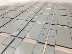
CoWoS is a 2.5D wafer-level multi-chip packaging technology that incorporates multiple dies side-by-side on a silicon interposer in order to achieve better interconnect density and performance. Individual chips are bonded through micro-bumps on a silicon interposer forming a chip-on-wafer (CoW). The CoW is then subsequently thinned such that the TSV perforations are exposed. This is followed C4 bumps formation and singulation. A CoWoS package is completed through bonding to a package substrate.
Versions[edit]
TSMC has introduced a number of versions since they first introduced the technology in 2012.
- CoWoS-1: First-generation CoWoS were primarily used for large FPGAs. CoWoS-1 had an interposer die area of up to ~800 mm², very close to reticle limit
- CoWoS-2: Second-generation of CoWoS increased the interposer size considerably through mask stitching. Originally qualified for 1200 mm², TSMC has since increased the interposer size to 1,700 mm². Those large packages are referred to as CoWoS-XL2.
| Year | Size (x reticle) | Options | Bandwidth |
|---|---|---|---|
| 2012 | 1.25x (~1070 mm²) | Logic+Logic | - |
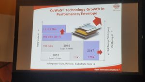
| 2016 | 1.5x (~1280 mm²) | Logic+Logic/HBM2 | 720 GB/s |
| 2017 | 1.75 (~1500 mm²) | Logic+Logic/HBM2 | 900 GB/s |
| 2019 | 1.85 (~1590 mm²) | Logic+Logic/HBM2 | 1 TB/s |
| 2020 | 2x (~1700 mm²) | Logic+Logic/HBM2E/3 | 2.7 TB/s |
| 2022 | 3x (~2500 mm²) | Logic+Logic/HBM3 | Up to 8.6 Tb/s |
Additional features[edit]
HK-MiM[edit]
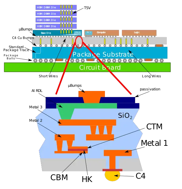
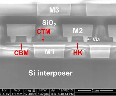
In 2014 TSMC detailed a high-K MiM. The high-K MiM was inserted between the Metal1 and Metal2 layers of the Si interposer. Since they are right in the interposer, they can effectively be used for system-level decoupling applications. At the time 1-, 2-, and 3- in-series decap combinations were discussed which provided a capacitance of 17.2, 4.3 and 1.9 fF/µm² respectively. With the HD-MiM, over an entire capacitor area of 200 mm², the HD-MiM can achieve a total capacitance of about 3.5 μF for the interposer die.
Integrated Capacitor (iCAP)[edit]
- See also: deep trench capacitor (DTC)
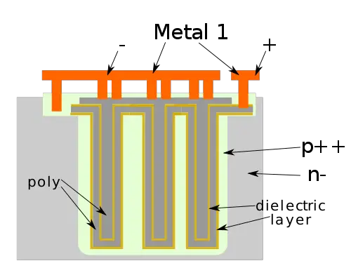
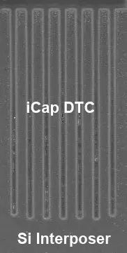
TSMC announced Integrated Capacitor (iCAP) in 2019. iCAPs are CoWoS deep trench capacitors with a standard cell of 40 µm by 40 µm. While TSMC was unwilling to disclose the depth of the trenches, the capacitance density it is able to achieve is up to 340 nF/mm². This translates to close to 20x improvement in capacitance density over the HD-MiM. Since multiple iCAPs can be used on a single interposer, the total capacitance possible is over 68 μF per Si interposer. iCAPs are high-yielding and have reported leakage currents below 1 fA/μm², including at high temperatures. TSMC reported very good PDN improvements with iCAP. Compared to equivalent CoWoS-based design without iCAP, TSMC is reporting just 0.05x the impedance and 0.45x the voltage droop.
Since both TSVs and DTCs co-exist on the same silicon wafer, there are two ways to construct iCAPs. In the DTC-first approach, the deep trenches are formed prior to the TSV process which means special care must be taken to ensure the TSV thermal budget does not impact the DTCs. Alternatively, in a TSV-first flow, the TSV structures are formed first using the standard TSV process, but special care must be taken to mitigate TSV related issues such as the via protrusion phenomenon. Like HD-MiMs, a major benefit of DTC over package decaps is that they can be freely placed as close as possible to the desired circuit similar to on-chip decaps but with the added benefit that the deep trenches allow for much higher capacitance. Additionally, since this can be implemented across an entire 1700 mm2 interposer with all kinds of chips on top, the DTCs can be more finely designed to better address the PI of the chip above it.
Industry[edit]
Examples[edit]
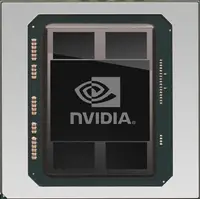
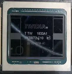
Nvidia Pascal P100:
- 16 nm SoC chip + 4 HBM2 (16 GB)
- 1200 mm² interposer
- 300 W TDP
- 150B transistors (15.3B SoC)
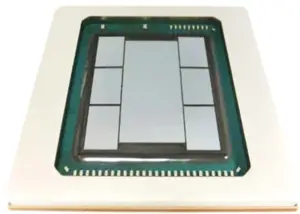
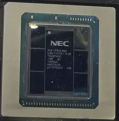
NEC Sx-Aurora:
- 16 nm process
- 60 mm x 60 mm (3600 mm²) package
- 32.5 mm x 38 mm (1235 mm²) interposer
- 15mm x 33mm (495 mm²) logic
- 300 W TDP
CoWoS-based Chips[edit]
- AMD Vega (7nm only)
- Barefoot Networks Template:barefoot
- Fujitsu A64FX
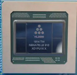
- Habana Labs Gaudi
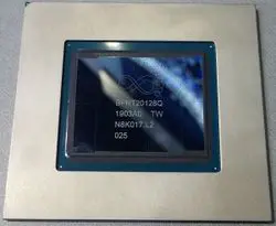
- Intel Spring Crest
- Nvidia Pascal
- Nvidia Volta
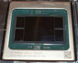
- NEC SX-Aurora
- Xilinx Virtex-7
- Xilinx Virtex UltraScale
This list is incomplete; you can help by expanding it.
Intel Nervana Spring Crest
Intel Habana Gaudi
NEC SX-Aurora
See also[edit]
Bibliography[edit]
- TSMC, 2013 IEEE 63rd Electronic Components and Technology Conference (ECTC).
- TSMC, 2014 IEEE 60th International Electron Devices Meeting (IEDM).
- TSMC, 2019 IEEE 65th International Electron Devices Meeting (IEDM).
