-
WikiChip
WikiChip
-
Architectures
Popular x86
-
Intel
- Client
- Server
- Big Cores
- Small Cores
-
AMD
Popular ARM
-
ARM
- Server
- Big
- Little
-
Cavium
-
Samsung
-
-
Chips
Popular Families
-
Ampere
-
Apple
-
Cavium
-
HiSilicon
-
MediaTek
-
NXP
-
Qualcomm
-
Renesas
-
Samsung
-
Integrated Connectivity (CNVi) is an architecture for wireless connectivity devices designed by Intel for their processors. CNVi was introduced in 2017 with the launch of Gemini Lake and is also planned for future mobile chipsets starting with Cannon Lake.
Overview
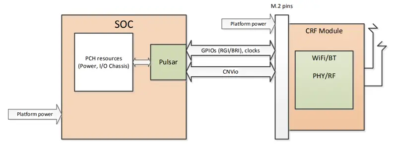
CNVi is an architecture for wireless connectivity designed by Intel for their recent mobile devices. Under the CNVi architecture, the large (and typically expensive) functional blocks found on a typical radio chip are moved onto the processor or chipset itself. This includes the processor and associated logic, memory, and the MAC components of the Bluetooth and Wi-Fi cores. The remaining parts (i.e., signal processor, analog and RF functions) are left on the Companion RF (CRF) module. This ultimately reduces the bill of material size and cost of the product.
The connectivity functionality that was moved to the SoC is incorporated in a block called a Pulsar. Pulsar interfaces with the rest of SoC through its internal interfaces and buses. Pulsar interfaces with the CRF module via the CNVio interface.
