Load-Line Calibration (LLC) is a mechanism offered to overclockers designed to compensate for large voltage droops when a CPU or GPU is under increased load. The mechanism attempts to compensate for the sudden sagging in voltage by preemptively applying additional voltage. The LLC, which is part of the voltage regulator module, was introduced in order to ensure a more smooth voltage delivery when the CPU/GPU is both idle as well as under heavy load, thereby eliminating related system instability or crashes on overclocked systems. This feature is aimed at overclockers as for normal systems the LLC is usually disabled by default because typical Vdroop is part of the system specification.
- Note: While extremely helpful at times, load-line calibration must be used with extreme care!
Overview
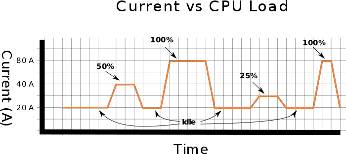
A modern computer system is never constant. To be more efficient and performant, the CPU will hop between very low and very high clock frequencies depending on how demanding the workload being executed is. Often this can be done very rapidly as the CPU is racing to sleep. When nothing is effectively being executed and the CPU is idle, the current is also relatively low. However, when the CPU is under load and the frequency shoots up, so will the current. An example graph is shown below.
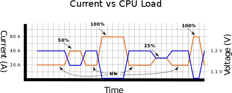
On a system with a static PWM Controller driving the voltage regulator module, the stored energy is constant. When the system goes from idle into being under load, there is no sufficient amount of energy to maintain the predefined voltage, causing a voltage drop. For example, a VRM operating at a constant 10% duty cycle delivering 1.2 V at idle will look like this:
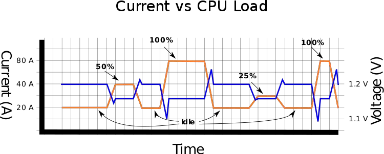
To prevent such drops, most modern VRMs have some form of feedback used to sense the voltage and current. When that happens, the circuits attempts to compensate for it by adjusting the duty cycle. For example, suppose the VRM that was previously shown dynamically adjusts to 12% duty cycle from 10% when it detects a drop, the voltage change would look similar to this:
It can be seen that the voltage under load is now considerably better than it was previously, allowing it to maintain a steady voltage for when it's both ideal and under load.
Overshoot
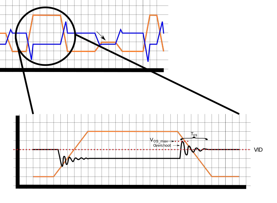
There is an obvious problem with this kind of technique and that is overshooting. When the PWM Controller senses added load and voltage drop, it will attempt to compensate for it by increasing the duty cycle. However, when the processor goes back to idle, since the controller cannot predict the future, there will be a delay until the PWM senses another drop and readjusts the duty cycle back down. Therefore, for a short period of time when the load current dropped, there will be a spike in voltage.
This spike, called an overshoot, exceeds the desired reference voltage. A spike in voltage that is too great will degrade the transistors on the chip. Extremely high voltage will cause a catastrophic breakdown of transistors. Companies such as Intel publish VRM specifications that specify what's the maximum allowed overshot voltage (VOS_max) and for how long it's allowed (TOS). Since motherboard manufacturers cannot exceed those ratings, there's a limit as to how high they can change the duty cycle before you exceed those ratings. Therefore it's natural for VRMs to have a certain amount of Vdroop in order to make sure they do not exceed the allowed overshoot voltage. In other words, Vdroop is intentionally added in order to prevent a voltage overshoot that is harmful to the CPU.


