Semiconductor & Computer Engineering
From WikiChip
File list
This special page shows all uploaded files.
First page |
Previous page |
Next page |
Last page |
| Date | Name | Thumbnail | Size | Description | Versions |
|---|---|---|---|---|---|
| 15:25, 31 May 2017 | kaby lake x (back).png (file) | .png) |
12 MB | Intel {{intel|Kaby Lake X|l=core}} Core chip, back. Image by Intel. | 1 |
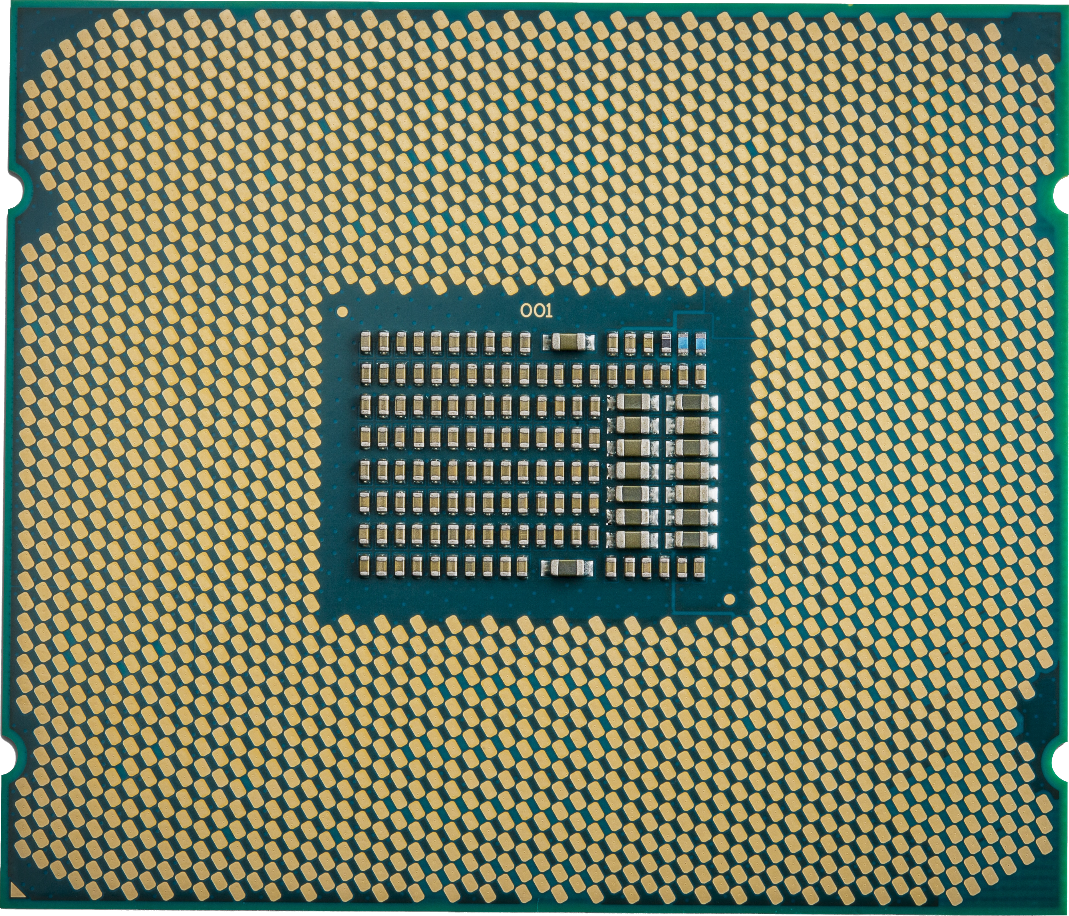
| 15:22, 31 May 2017 | skylake x (back).png (file) | .png) |
19.8 MB | corrected image | 2 |
| 07:04, 27 May 2017 | skylake decode.svg (file) |  |
28 KB | should be 5 not 6 paths | 6 |
| 14:57, 18 May 2017 | power8 die shot (6-core)(annotated).png (file) | (annotated).png) |
1.09 MB | Annotated IBM {{ibm|POWER8|l=arch}} 6 cores die shot by IBM. | 1 |
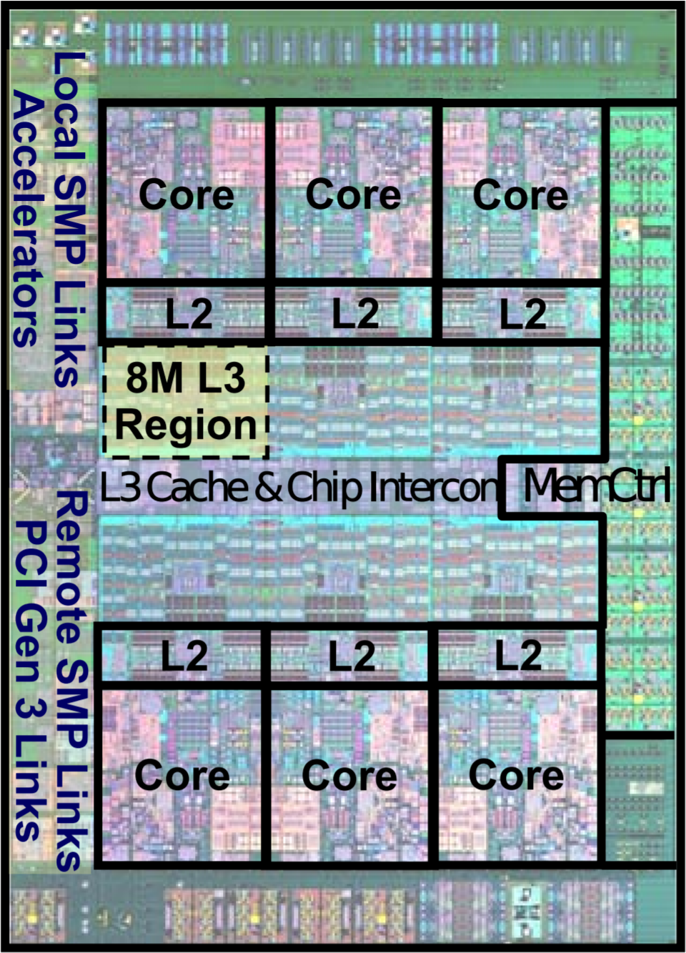
| 13:56, 18 May 2017 | power8 die shot (12-core)(annotated).png (file) | (annotated).png) |
7.82 MB | Annotated version by WikiChip of the IBM {{ibm|POWER8|l=arch}} 12 cores die shot by IBM. * Original version: File:power8 die shot (12-core).png | 1 |
| 10:42, 18 May 2017 | power8 die shot (12-core).png (file) | .png) |
10.33 MB | IBM {{ibm|POWER8|l=arch}} 12 cores die shot by IBM. | 1 |
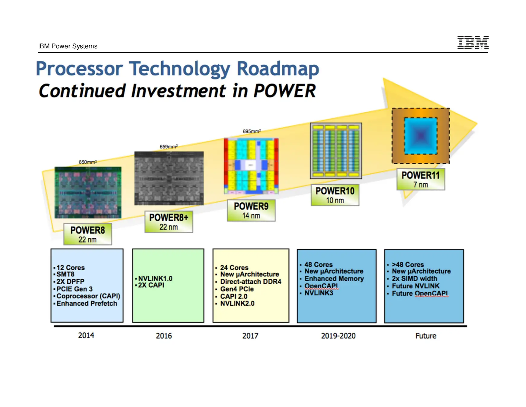
| 10:25, 18 May 2017 | ibm power9-11 roadmap.png (file) |  |
860 KB | IBM {{ibm|POWER9|l=arch}} through {{ibm|POWER11|l=arch}} roadmap. | 1 |
| 15:17, 15 May 2017 | skylake u (front; standard).png (file) | .png) |
12.31 MB | Intel {{intel|Skylake|l=arch}} chip, FCLGA-1356 package. Image by Intel. | 1 |
| 14:09, 15 May 2017 | skylake (fclga1515).png (file) | .png) |
4.02 MB | Intel {{intel|Skylake|l=arch}} chip, FCLGA-1515 package. Image by Intel. | 1 |
| 01:17, 15 May 2017 | skylake s (front).png (file) | .png) |
36.85 MB | Front of {{intel|Skylake S|l=core}} package by Intel Press. Copyright of Intel. | 1 |
| 01:17, 15 May 2017 | skylake s (back).png (file) | .png) |
52.99 MB | Back of {{intel|Skylake S|l=core}} package by Intel Press. Copyright of Intel. | 1 |
| 20:02, 14 May 2017 | skylake (fclga1151).png (file) | .png) |
1.07 MB | Inte {{intel|Skylake|l=arch}} chip, FCLGA-1151 package. Image by Intel. | 1 |
| 03:28, 12 May 2017 | tech node naming.svg (file) | 91 KB | 4 | ||
| 19:04, 8 May 2017 | Intel Architecture, Code Name Skylake Deep Dive- A New Architecture to Manage Power Performance and Energy Efficiency.pdf (file) |  |
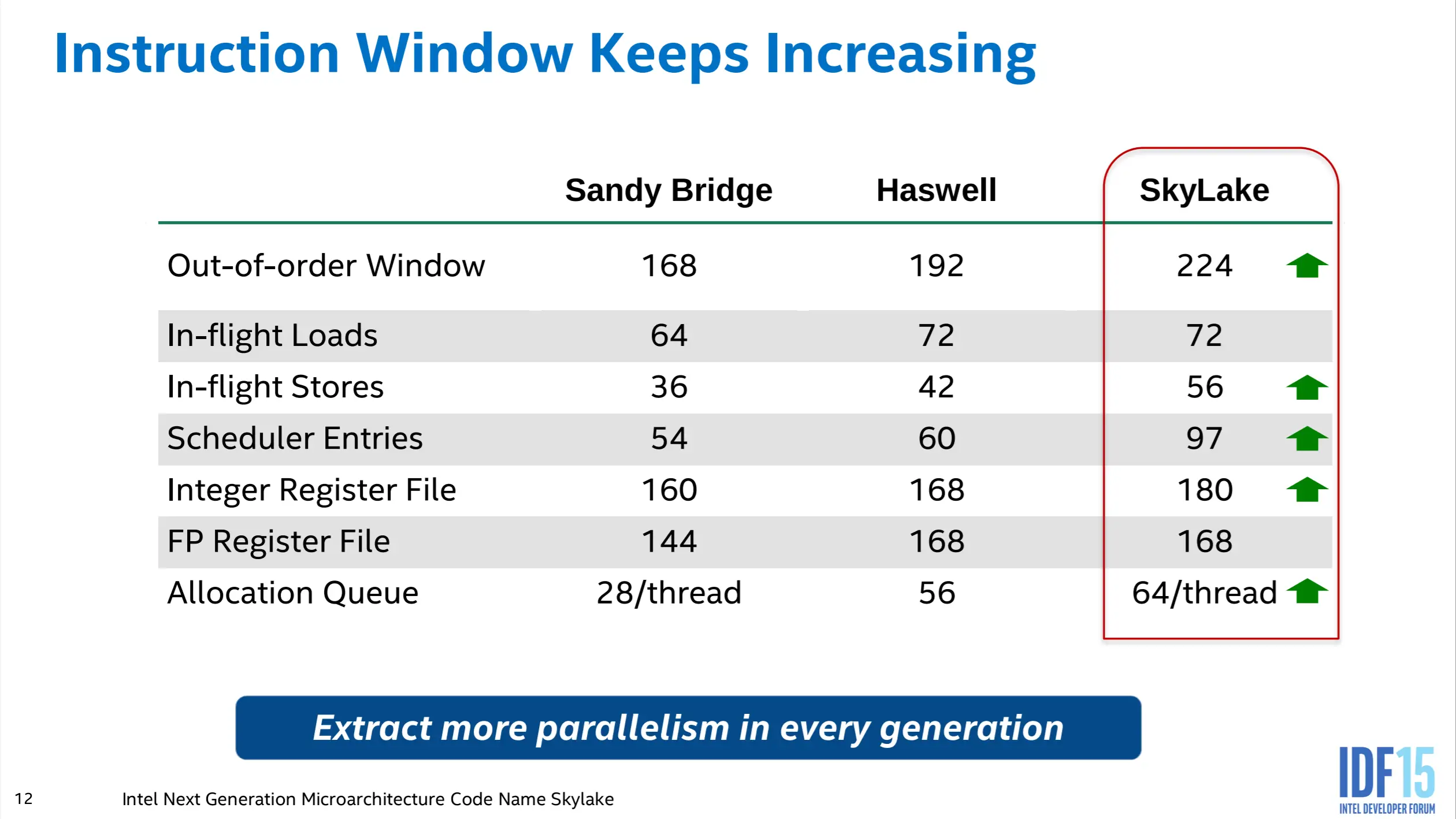
1.88 MB | Intel {{intel|Skylake|l=arch}} Power, Intel IDF 2015 | 1 |
| 18:54, 8 May 2017 | Technology Insight Intel’s Next Generation Microarchitecture Code Name Skylake.pdf (file) |  |
3.78 MB | Intel {{intel|Skylake|l=arch}} IDF 2015 | 1 |
| 17:25, 8 May 2017 | skylake ipu.png (file) | 183 KB | Intel {{intel|Skylake|l=arch}} Image Processing Unit | 1 | |
| 22:14, 7 May 2017 | skylake buff window.png (file) |  |
306 KB | Intel {{intel|Skylake|l=arch}} Buffer Windows by Intel | 1 |
| 10:26, 6 May 2017 | skylake scheduler.svg (file) |  |
52 KB | 5 | |
| 23:30, 5 May 2017 | skylake mem subsystem.svg (file) |  |
27 KB | 2 | |
| 20:39, 5 May 2017 | skylake ucache.svg (file) |  |
30 KB | moved the mux to after the ucache because made it seem like it can bypass it, which is wrong. | 2 |
| 20:38, 4 May 2017 | kaby lake soc block diagram (dual).svg (file) | .svg) |
25 KB | My drawing of {{intel|Kaby Lake|l=arch}} SOC in a block diagram. Dual core SoC. | 1 |
| 20:38, 4 May 2017 | skylake soc block diagram (dual).svg (file) | .svg) |
24 KB | My drawing of {{intel|Skylake|l=arch}} SOC in a block diagram. Dual core SoC. | 1 |
| 20:31, 4 May 2017 | kaby lake soc block diagram.svg (file) |  |
27 KB | 3 | |
| 20:30, 4 May 2017 | skylake soc block diagram.svg (file) |  |
30 KB | another try | 4 |
| 01:18, 4 May 2017 | skylake rob.svg (file) |  |
24 KB | Intel {{intel|Skylake|l=arch}} arch ROB | 1 |
| 12:52, 1 May 2017 | core mopf on.png (file) |  |
251 KB | 2 | |
| 12:52, 1 May 2017 | core mopf off.png (file) |  |
255 KB | 2 | |
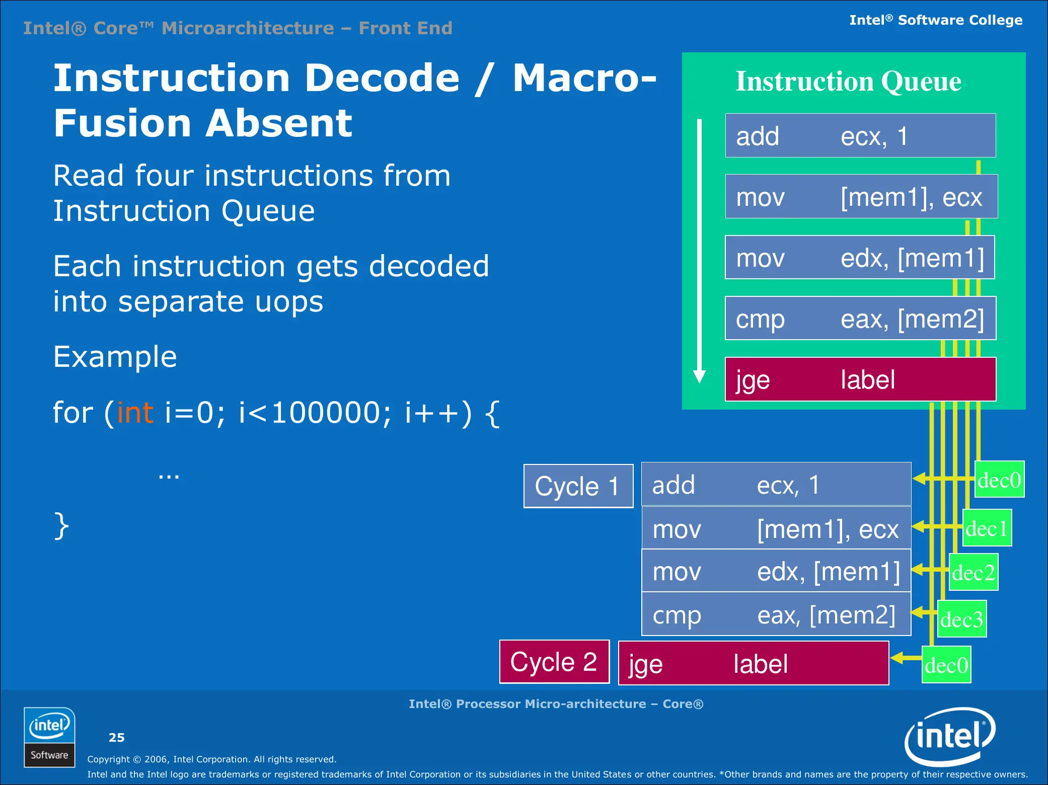
| 00:58, 1 May 2017 | 01-2 Intel C2 AE Processor Architecture-Core.ppt (file) | 1.66 MB | [[Intel]® Processor Micro-architecture – {{intel|Core|l=arch}}® Intel® Software College 2006 | 1 | |
| 19:41, 30 April 2017 | nehalem die shot.png (file) |  |
8.87 MB | Intel {{intel|Nehalem|l=arch}} die shot by Intel. Copyright Intel. | 1 |
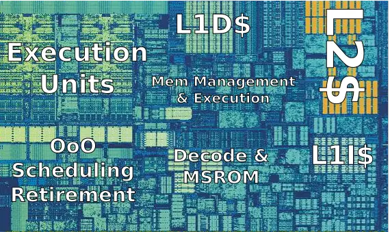
| 19:14, 30 April 2017 | skylake core die (annotated).png (file) | .png) |
522 KB | removed the shading, it was distracting | 3 |
| 19:12, 30 April 2017 | skylake core die.png (file) |  |
564 KB | rotated version | 2 |
| 19:40, 29 April 2017 | skylake 4x core complex die.png (file) |  |
5.46 MB | Intel {{intel|Skylake|l=arch}} 4x core complex from a dual-core die shot by Intel. | 1 |
| 17:42, 29 April 2017 | skylake 2x core complex die.png (file) |  |
1.51 MB | Intel {{intel|Skylake|l=arch}} 2x core complex from a dual-core die shot by Intel. | 1 |
| 18:19, 28 April 2017 | skylake fetch.svg (file) |  |
15 KB | typo | 4 |
| 17:41, 20 April 2017 | zen block diagram.svg (file) |  |
111 KB | a few more corrected details | 14 |
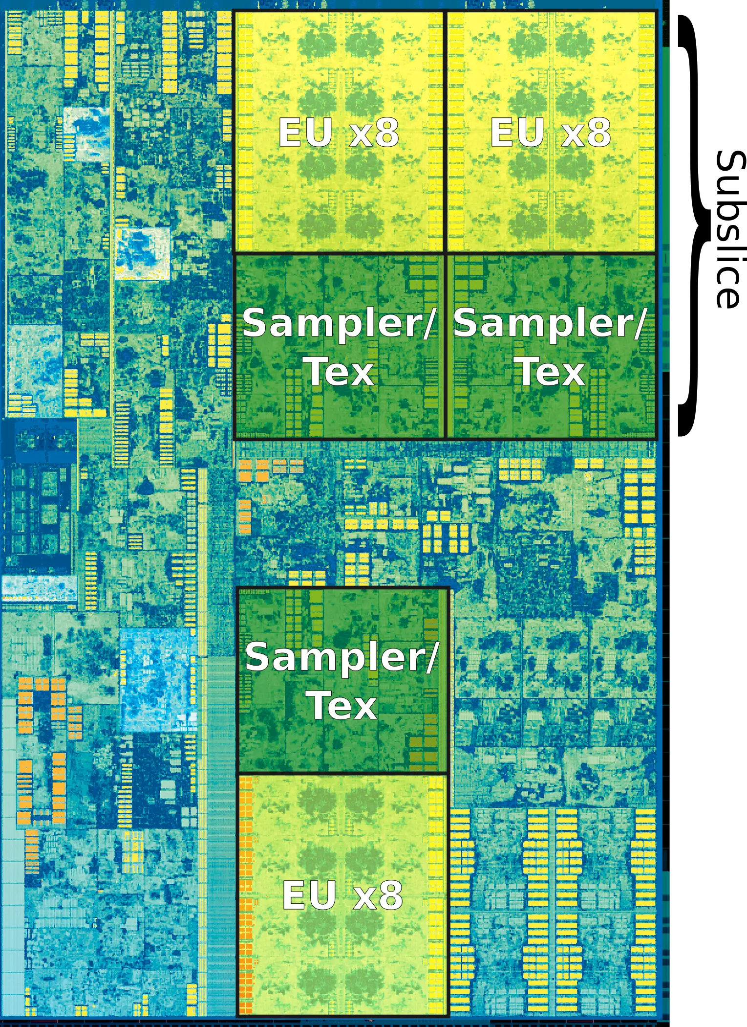
| 16:04, 18 April 2017 | kaby lake gpu.png (file) |  |
6.17 MB | GPU area of the {{intel|Kaby Lake|l=arch}} die shot. * Annotated Version: File:kaby lake gpu (annotated).png | 1 |
| 16:04, 18 April 2017 | kaby lake gpu (annotated).png (file) | .png) |
5.7 MB | GPU area of the {{intel|Kaby Lake|l=arch}} die shot. Annotated Version by WikiChip. * Annotated Version: File:kaby lake gpu.png | 1 |
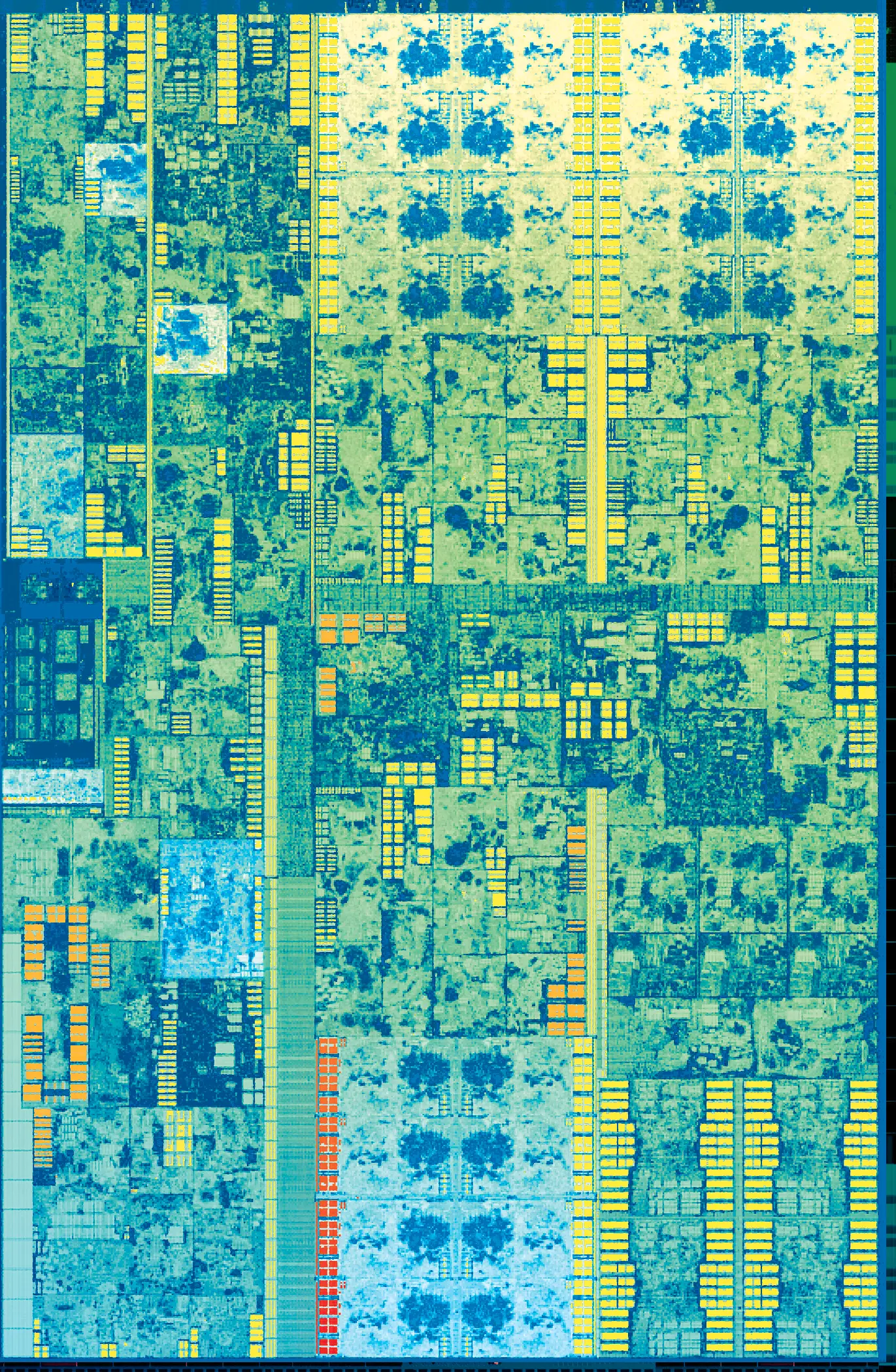
| 21:01, 17 April 2017 | kaby lake 4c sa.png (file) |  |
2.11 MB | Intel's {{intel|Kaby Lake|l=arch}} System Agent for the 4-core die. * Annotated Version: File:kaby lake 4c sa (annotated).png | 1 |
| 21:01, 17 April 2017 | kaby lake 4c sa (annotated).png (file) | .png) |
1.71 MB | Intel's {{intel|Kaby Lake|l=arch}} System Agent for the 2-core die. * Original Version: File:kaby lake 4c sa.png | 1 |
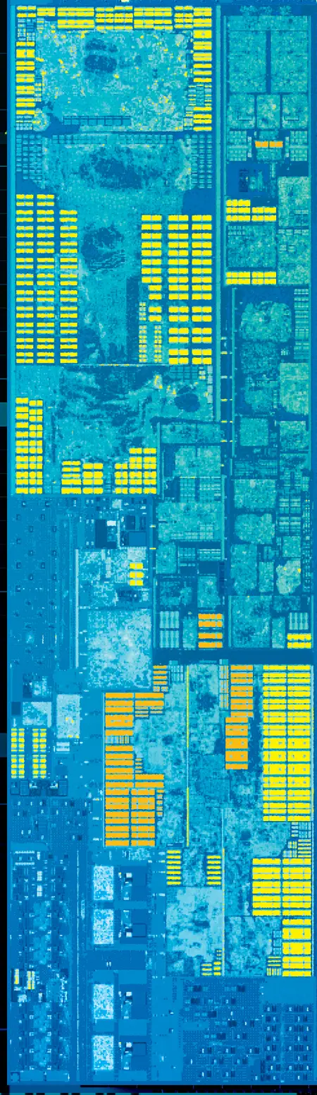
| 19:06, 17 April 2017 | kaby lake 2c sa.png (file) |  |
1.42 MB | Intel's {{intel|Kaby Lake|l=arch}} System Agent for the 2-core die. * Annotated version: File:kaby_lake_2c_sa_(annotated).png | 1 |
| 19:04, 17 April 2017 | kaby lake 2c sa (annotated).png (file) | .png) |
1.08 MB | text | 2 |
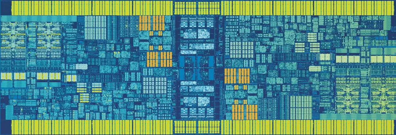
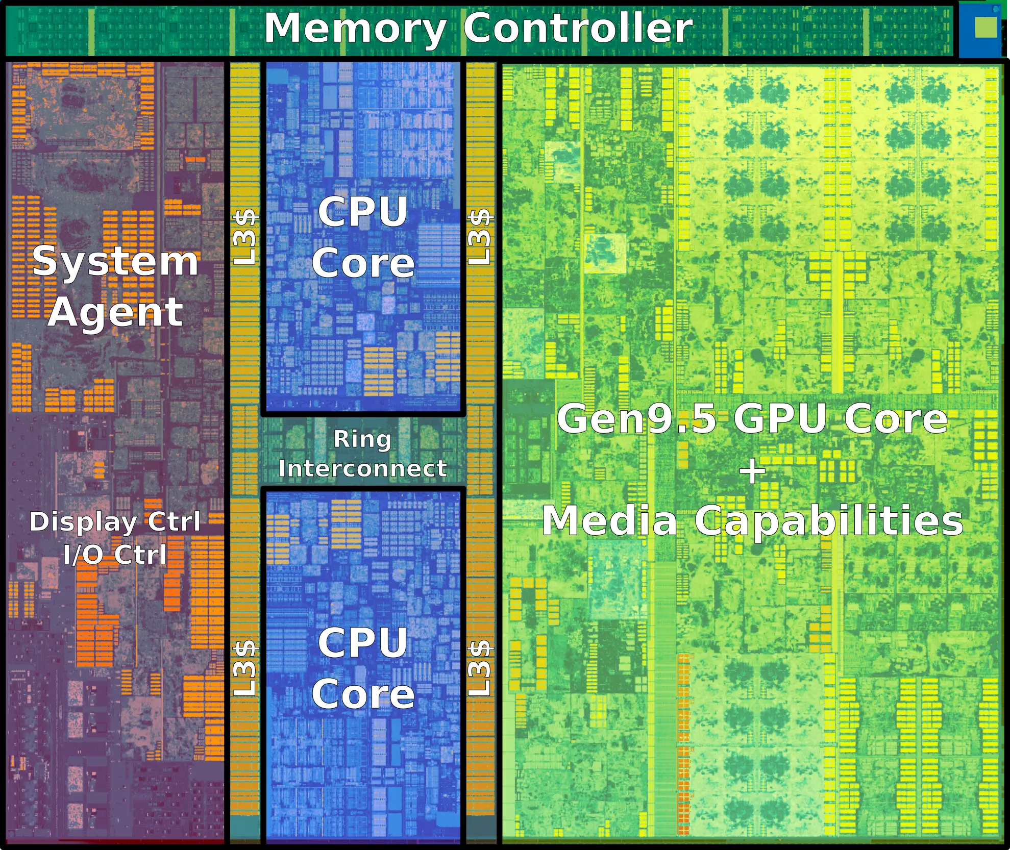
| 01:14, 17 April 2017 | kaby lake (quad core) (annotated).png (file) | _(annotated).png) |
12.16 MB | larger fonts | 3 |
| 00:33, 17 April 2017 | kaby lake (dual core) (annotated).png (file) | _(annotated).png) |
5.61 MB | Spelling | 3 |
| 08:01, 14 April 2017 | AMD-Ryzen-Processor-and-AMD-Ryzen-Master-Overclocking-Users-Guide.pdf (file) |  |
1.42 MB | AMD {{amd|Ryzen}} processors Master Overclocking User Guide | 1 |
| 08:00, 14 April 2017 | amd-ryzen-cpu-optimization.pdf (file) |  |
1.87 MB | AMD {{amd|Ryzen}} CPU Optimization | 1 |
| 05:50, 14 April 2017 | zen soc clock domain.svg (file) |  |
64 KB | clock unicode symbol were not displaying correctly, converted them to paths | 2 |
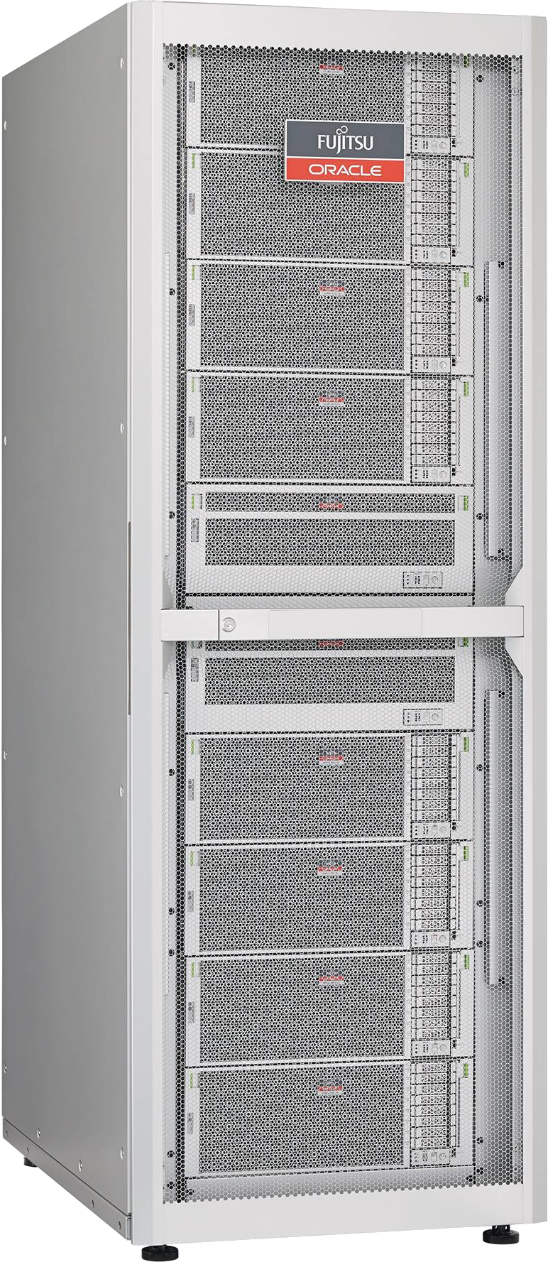
| 22:52, 12 April 2017 | m12-2s.png (file) |  |
2.18 MB | Fujitsu M12-2S server employing the {{fujitsu|SPARC64 XII}} microprocessor. Copyright Fujitsu. | 1 |
| 22:38, 12 April 2017 | sparc64 xii wafer.jpg (file) |  |
275 KB | Fujitsu {{fujitsu|SPARC64 XII}} wafer by Fujitsu. Copyright Fujitsu. | 1 |
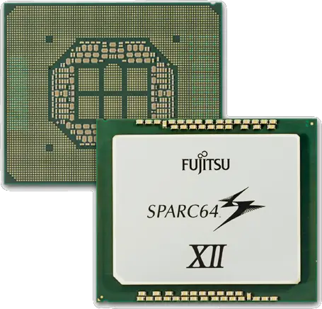
| 22:25, 12 April 2017 | sparc64 xii.png (file) |  |
299 KB | Fujitsu {{fujitsu|SPARC64 XII}} | 1 |
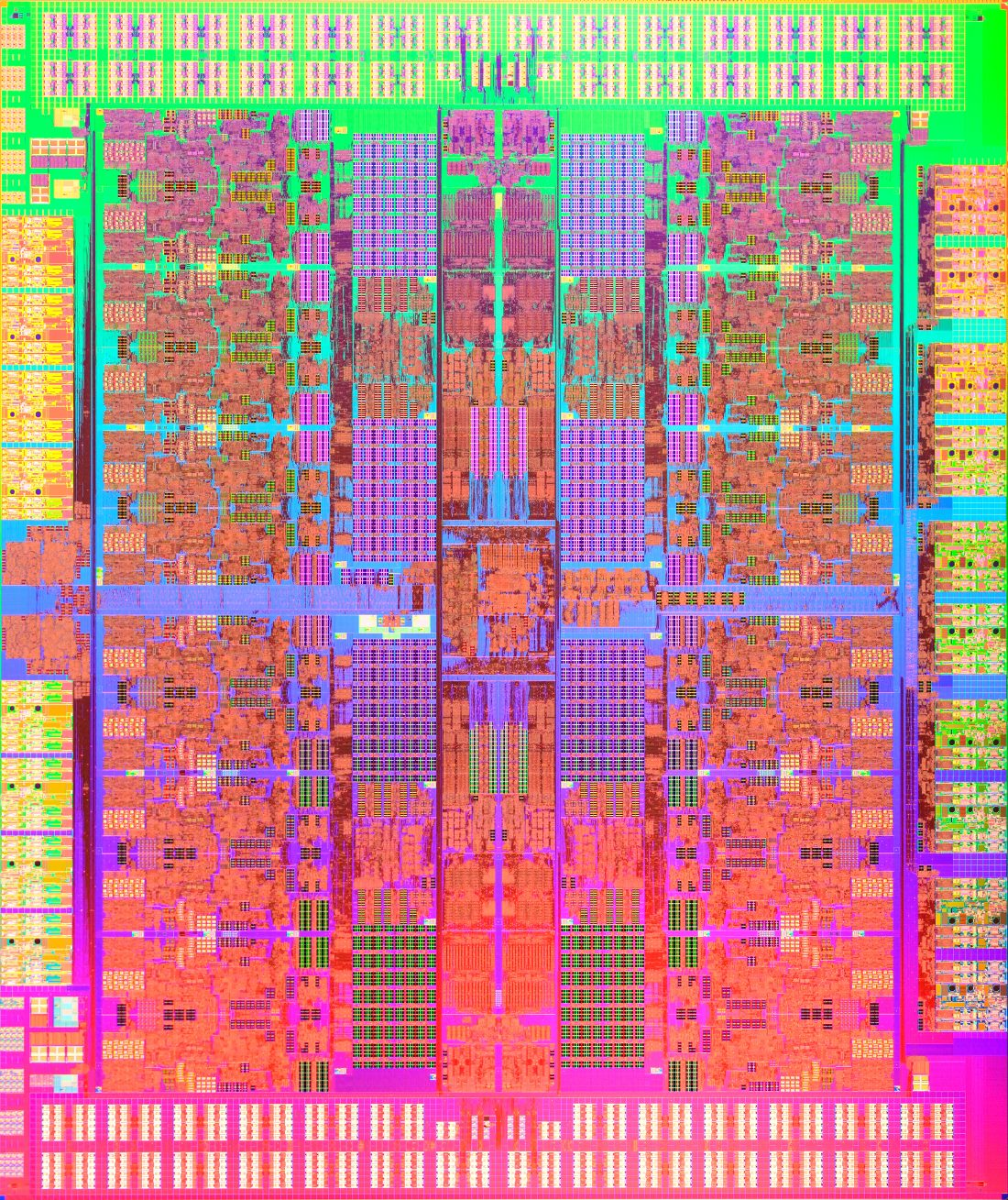
| 22:21, 12 April 2017 | sparc64 xii die shot.png (file) |  |
3.13 MB | Die shot of {{fujitsu|SPARC64 XII}} by Fujitsu. Copyright Fujitsu. * Annotated version: File:sparc64_xii_die_shot_(annotated).png | 1 |
.png)
First page |
Previous page |
Next page |
Last page |