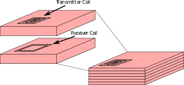
Template:3d integration ThruChip Interface (TCI) is a high-performance wireless vertical interconnect technology used to transmit signals between multiple stacked dies. TCI is an alternative technology to through-silicon via.
Overview
ThruChip Interface splits up the problem of vertical interconnects into two separate problems: data communication and power distribution. For data communication, TCI uses a wireless near-field inductive coupling. Since the data is separate from the power distribution solution, solving the aspect of power is fairly trivial in one of the many solutions such as wire bond, RDL, and TSV. For ThruChip in particular, the recommended solution is highly-doped silicon via (HDSV).
Under normal circumstances, chip designers try to avoid forming too much coupling between wires. TCI attempts to leverage this problem to from inductors which can then be used to communicate with a coil stacked above and below the current die. Communication can extend to a whole stack of dies. TCI relies on highly-advanced wafer thinning process capable of providing sub-10µm thick wafers. Because the diameter of the inductor is roughly three times the vertical communication distance, with ultra-thin wafers the inductors can shrink quietly substantially. It's worth noting that since TCI uses a magnetic field for communication, the coils can then be placed on some top layer (above logic, power rails, etc..) which will permeate through all the layers, including the silicon itself, without affecting the rest of the circuit.
Comparison to TSV
Compared to through-silicon via, TCI can offer considerably higher bandwidth at lower power, less area, and at much lower costs. The power and cost come from the fact that TCI, unlike TSV, uses the base CMOS process unmodified without any added steps.
TCI uses 30% less I/O compared to LPDDR4 and 0.83% less I/O compared to TSV while offering twice the data rate of LPDDR4 at lower I/O interface area. Additionally, since there are no through holes in the silicon, there is no degradation in yield and no modification to the base process.
Operation
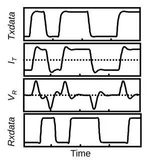
Coupling is done by a magnetic field. Very little voltage is required in practice to pass a magnetic field through silicon, transistors, and metal layers. This can be constructed using a simple H-bridge configuration where the slew rate is your generated voltage pulse rate, getting latched in the receiver following some fixed number of gate delay.
Security Concern
An area of concern with TCI has been the ability to pick up on the transmission. Near field signals decay very rapidly, inversely proportional to the distance cubed. Meaning they can only reach very short distances. It is possible to cap those signals at the ends of the transmission lines, albeit further research is likely necessary to be the issue to rest.
References
- IEEE Hot Chips 26 Symposium (HCS) 2014
- IEEE IEDM 2014


