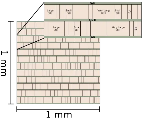
MTr/mm² (mega-transistor per squared millimeter) is a transistor density unit that serves as a figure of merit in quantifying a process node. The metric makes use of a weighted system consisting of two typical standard cells found in most libraries - a very small NAND2 cell and a very large SFF cell.
Contents
History
The metric is actually a resurrection of similar variants that were sparsely used and abandoned over time. The metric was formally proposed by Mark Bohr, Intel's director of process architecture and integration, in 2017, although similar analysis have been done by various individuals and organizations prior to his formalization.
Overview
As the semiconductor industry evolved, device scaling over the last decade extended well beyond the individual transistors. With the introduction of scaling boosters a more comprehensive metric was necessary in order to evaluate the density of a given process node. This metric attempts to take into account second-order design rules that the simpler density metrics such as CPP x MxP and CPP x MxP x Tracks cannot capture because they do not represent a typical standard cell. This metrics estimates the transistor density of an integrated circuit by filling a square die with cells from north to south and all the way from west to east with a combination of large and small cells in order to provide a realistic density estimate.
It should be noted that the metric explicitly excludes SRAM cell sizes because of the large variance in SRAM-to-logic ratio between popular chips. Furthermore, the metal pitch does not play a role in limiting SRAM as it does with other standard cells. Therefore, SRAM cell sizes should be reported separately alongside the MTr/mm² unit.
Two cells that are universally found in every standard library are used: a very small 2-input NAND cell consisting of just four transistors and a very large scan flip-flop cell. The NAND2 is weighted as 0.6 while the SFF is weighted as 0.4.
Advantages
The major advantage of this metric over most other alternatives is that it offers an apples-to-apples comparison of digital CMOS transistors at the cell-level. Where's previous metrics such as CPP x MxP and CPP x MxP x Tracks could not properly capture cell-level optimization, this metric is able to take those features into account.
There are a number of shortcomings to this metric. Actual SoCs have to deal with hot spots that require spacers and spacing out high-performance regions of the chip which reduces the realized density. Since the density of analog transistors is seldom disclosed, they are not taken into account either with this metric. Additionally, due to the variations in the usage of SRAM in modern SoCs, they are not included either. Because SRAM cells are considerably more dense than standard cells, a larger amount of SRAM will inflate the transistor count.
Example
Intel's 10 nm process consists of a minimum metal pitch of 36nm with 8 diffusion lines for a cell height of 272 nanometers. Additionally, the process has a poly pitch of 54 nm and cells on Intel's 10 nm use a single dummy gate. For 0.6 NAND2 + 0.4 SFF, Intel's 10nm has a density of 100.76 MTr/mm² along with a high-density 6T SRAM measuring 0.0312 µm². Note that Intel itself reported their 10nm at 100.8 MTr/mm².
Intel's 22 nm process (2012) had 16.5 MTr/mm², 14 nm process (2014) had 44.67 MTr/mm², and 14++ nm process had 37.22 MTr/mm².

