Semiconductor & Computer Engineering
| Packaging | |
 | |
| Technologies | |
| Concepts | |
| Single-Row | |
| Dual-Row | |
| Quad-Row | |
| Grid Array | |
| 2.5D IC | |
| 3D IC | |
Chip-on-Wafer-on-Substrate (CoWoS) is a two-point-five dimensional integrated circuit (2.5D IC) through-silicon via (TSV) interposer-based packaging technology designed by TSMC for high-performance applications.
Overview
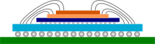
CoWoS is a 2.5D wafer-level multi-chip packaging technology that incorporates multiple dies side-by-side on a silicon interposer in order to achieve better interconnect density and performance. Individual chips are bonded through micro-bumps on a silicon interposer forming a chip-on-wafer (CoW). The CoW is then subsequently thinned such that the TSV perforations are exposed. This is followed C4 bumps formation and singulation. A CoWoS package is completed through bonding to a package substrate.
Versions
TSMC has introduced a number of versions since they first introduced the technology in 2012.
CoWoS-1
First-generation CoWoS were primarily used for large FPGAs. CoWoS-1 had an interposer die area of up to ~800 mm², very close to reticle limit
CoWoS-2
Second-generation of CoWoS increased the interposer size considerably through mask stitching. Originally qualified for 1200 mm², TSMC has since increased the interposer size to 1,700 mm². Those large packages are referred to as CoWoS-XL2.
Examples
Nvidia Pascal P100:
- 16 nm SoC chip + 4 HBM2 (16 GB)
- 1200 mm² interposer
- 300 W TDP
- 150B transistors (15.3B SoC)


NEC Sx-Aurora:
- 16 nm process
- 60 mm x 60 mm (3600 mm²) package
- 32.5 mm x 38 mm (1235 mm²) interposer
- 15mm x 33mm (495 mm²) logic
- 300 W TDP

