Semiconductor & Computer Engineering
(added a device name that contain this cpu) |
|||
| (92 intermediate revisions by 58 users not shown) | |||
| Line 1: | Line 1: | ||
{{qualcomm title|Snapdragon 855}} | {{qualcomm title|Snapdragon 855}} | ||
{{chip | {{chip | ||
| − | |name=Snapdragon 855 | + | |name=Qualcomm Snapdragon 855 |
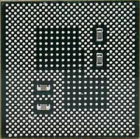
|image=sd 855 (front).png | |image=sd 855 (front).png | ||
|back image=sd 855 (back).png | |back image=sd 855 (back).png | ||
| Line 7: | Line 7: | ||
|designer 2=ARM Holdings | |designer 2=ARM Holdings | ||
|manufacturer=TSMC | |manufacturer=TSMC | ||
| + | |model number=SDM855 | ||
| + | |part number=SM8150 | ||
|market=Mobile | |market=Mobile | ||
|first announced=December 4, 2018 | |first announced=December 4, 2018 | ||
| − | |first launched= | + | |first launched=March, 2019 |
|family=Snapdragon 800 | |family=Snapdragon 800 | ||
|series=800 | |series=800 | ||
| + | |frequency=1,800 MHz | ||
| + | |frequency 2=2,420 MHz | ||
| + | |frequency 3=2,840 MHz | ||
|isa=ARMv8 | |isa=ARMv8 | ||
|isa family=ARM | |isa family=ARM | ||
| Line 19: | Line 24: | ||
|core name 2=Kryo 485 Silver | |core name 2=Kryo 485 Silver | ||
|process=7 nm | |process=7 nm | ||
| + | |transistors=6,700,000,000 | ||
|technology=CMOS | |technology=CMOS | ||
| + | |die area=73.27 mm² | ||
| + | |die length=8.48 mm | ||
| + | |die width=8.64 mm | ||
|word size=64 bit | |word size=64 bit | ||
|core count=8 | |core count=8 | ||
|thread count=8 | |thread count=8 | ||
| + | |max memory=16 GiB | ||
|max cpus=1 | |max cpus=1 | ||
| − | |||
|predecessor=Snapdragon 845 | |predecessor=Snapdragon 845 | ||
|predecessor link=qualcomm/snapdragon 800/845 | |predecessor link=qualcomm/snapdragon 800/845 | ||
| + | |successor=Snapdragon 865 | ||
| + | |successor link=qualcomm/snapdragon_800/865 | ||
| + | |contemporary=Snapdragon 855+/860 | ||
| + | |contemporary link=qualcomm/snapdragon_800/855 plus | ||
}} | }} | ||
[[File:snapdragon-855-block-diagram.png|thumb|right|Block Diagram|200px]] | [[File:snapdragon-855-block-diagram.png|thumb|right|Block Diagram|200px]] | ||
| − | '''Snapdragon 855''' is a high-performance {{arch|64}} [[ARM]] [[LTE]] [[system on a chip]] designed by [[Qualcomm]] and introduced in late [[2018]]. Fabricated on | + | '''Snapdragon 855''' is a high-performance {{arch|64}} [[ARM]] [[LTE]] [[system on a chip]] designed by [[Qualcomm]] and introduced in late [[2018]]. Fabricated on [[N7|TSMC 7nm process]], the 855 features four [[Kryo 485 Silver]] high-efficiency cores operating at 1.8 GHz along with three high-performance [[Kryo 485 Gold]] operating at 2.42 GHz and another higher-performance [[Kryo 485 Gold]] core operating at 2.84 GHz. The Snapdragon 855 integrates the {{qualcomm|Adreno 640}} [[GPU]] operation at 585 MHz and features an X24 LTE modem supporting Cat 20 uplink and Cat 20 downlink. This chip supports up to 16 GiB of quad-channel LPDDR4X-4266 memory. |
The Snapdragon 855 can be paired with Qualcomm's X50 5G modem (an external chip) and an RF front-end interface chip (RFFE) to bring 5G NR, sub-6 GHz and mmWave, support. | The Snapdragon 855 can be paired with Qualcomm's X50 5G modem (an external chip) and an RF front-end interface chip (RFFE) to bring 5G NR, sub-6 GHz and mmWave, support. | ||
| + | |||
| + | The {{\\|855 Plus}} is an identical, but higher clocked version of this processor. | ||
| + | |||
| + | == Clock domains == | ||
| + | {{see also|7 nm lithography process#N7|l1=TSMC 7-nanometer (N7) process technology}} | ||
| + | The Snapdragon 855 utilizes TSMC [[N7|7-nanometer]] process. One of the major changes Qualcomm has done compared to the [[Snapdragon 845]] is on the physical implementation side. Whereas the Snapdragon 845 uses two clock domains in a standard [[DynamIQ]] cluster - one for the Silver cores and one for the Gold cores, the 855 uses three clock domains. One of the cores from the prior quad-core Gold clock domains has been moved to its own clock domain. Qualcomm refers to that core as a 'Prime' core. The Prime core utilizes TSMC high-performance cell (which uses a slightly relaxed 64 nm poly pitch) while the rest of the SoC utilizes TSMC standard high-density cells. The use of the high-performance [[standard cell|cells]] allows for the slightly higher frequency at similar power. | ||
| + | |||
| + | |||
| + | [[File:sdm855-clocks.svg|500px]] | ||
| + | |||
| + | |||
| + | Qualcomm reported that at the same power, Clock2 CPUs have improved by roughly 20% from the SDM845 to the SDM855. With the addition of Clock3, the four cores collectively extend this performance gain over the quad-core cluster on the 845 to over 30%. Check New [https://www.dopetechnews.com/Comparison/qualcomm-snapdragon-8-gen-1-vs-a15-bionic/ Qualcomm Snapdragon 8 gen 1 vs A15 Bionic] Comparison | ||
| + | |||
| + | |||
| + | [[File:855 clock improvement.png|550px]] | ||
| + | |||
| + | == Cache == | ||
| + | {{main|arm_holdings/microarchitectures/cortex-a76#Memory_Hierarchy|arm_holdings/microarchitectures/cortex-a55#Memory_Hierarchy|l1=Cortex-A76 § Cache|l2=Cortex-A55 § Cache}} | ||
| + | |||
| + | Prime core {{armh|Cortex-A76|l=arch}}: | ||
| + | {{cache size | ||
| + | |l1 cache=128 KiB | ||
| + | |l1i cache=64 KiB | ||
| + | |l1i break=1x64 KiB | ||
| + | |l1i desc=4-way set associative | ||
| + | |l1d cache=64 KiB | ||
| + | |l1d break=1x64 KiB | ||
| + | |l1d desc=4-way set associative | ||
| + | |l2 cache=512 KiB | ||
| + | |l2 break=1x512 KiB | ||
| + | |l2 desc=8-way set associative | ||
| + | }} | ||
| + | |||
| + | 3 core cluster {{armh|Cortex-A76|l=arch}}: | ||
| + | {{cache size | ||
| + | |l1 cache=384 KiB | ||
| + | |l1i cache=192 KiB | ||
| + | |l1i break=3x64 KiB | ||
| + | |l1i desc=4-way set associative | ||
| + | |l1d cache=192 KiB | ||
| + | |l1d break=3x64 KiB | ||
| + | |l1d desc=4-way set associative | ||
| + | |l2 cache=768 KiB | ||
| + | |l2 break=3x256 KiB | ||
| + | |l2 desc=8-way set associative | ||
| + | }} | ||
| + | |||
| + | Quad-core cluster {{armh|Cortex-A55|l=arch}}: | ||
| + | {{cache size | ||
| + | |l1 cache=512 KiB | ||
| + | |l1i cache=256 KiB | ||
| + | |l1i break=4x64 KiB | ||
| + | |l1i desc=2-way set associative | ||
| + | |l1d cache=256 KiB | ||
| + | |l1d break=4x64 KiB | ||
| + | |l1d desc=4-way set associative | ||
| + | |l2 cache=512 KiB | ||
| + | |l2 break=4x128 KiB | ||
| + | |l2 desc=8-way set associative | ||
| + | }} | ||
| + | |||
| + | * 2 MiB L3 | ||
== Memory controller == | == Memory controller == | ||
| Line 39: | Line 114: | ||
|max mem=16 GiB | |max mem=16 GiB | ||
|controllers=1 | |controllers=1 | ||
| − | |channels= | + | |channels=4 |
|width=16 bit | |width=16 bit | ||
|max bandwidth=31.79 GiB/s | |max bandwidth=31.79 GiB/s | ||
| Line 50: | Line 125: | ||
== DSP == | == DSP == | ||
{{#set: dsp|Hexagon 690 DSP}} | {{#set: dsp|Hexagon 690 DSP}} | ||
| − | This chip features [[Qualcomm]]'s {{qualcomm|Hexagon}} {{qualcomm|Hexagon | + | This chip features [[Qualcomm]]'s {{qualcomm|Hexagon}} {{qualcomm|Hexagon 690|690}} DSP. |
== Graphics == | == Graphics == | ||
| Line 56: | Line 131: | ||
| gpu = Adreno 640 GPU | | gpu = Adreno 640 GPU | ||
| designer = Qualcomm | | designer = Qualcomm | ||
| − | | execution units = | + | | execution units = 2 (384x2 ALU) |
| max displays = 2 | | max displays = 2 | ||
| max memory = | | max memory = | ||
| − | | frequency = | + | | frequency = 257 MHz |
| − | | max frequency = | + | | max frequency = 585 MHz |
| output crt = | | output crt = | ||
| Line 100: | Line 175: | ||
*** Hardware accelerator for computer vision (CV-ISP) | *** Hardware accelerator for computer vision (CV-ISP) | ||
** Up to 20 MP dual camera | ** Up to 20 MP dual camera | ||
| − | ** Up to | + | ** Up to 48 MP single camera |
* Photo Capture: HEIF photo capture | * Photo Capture: HEIF photo capture | ||
| Line 127: | Line 202: | ||
* WiFi | * WiFi | ||
| − | ** Standards: 802. | + | ** Standards: 802.11ax, 802.11ac Wave 2, 802.11a/b/g, 802.11n |
| − | ** Spectral Bands: 2.4 GHz, 5 | + | ** Spectral Bands: 2.4 GHz, 5 GHz |
* Bluetooth | * Bluetooth | ||
| Line 136: | Line 211: | ||
== Location == | == Location == | ||
* Systems: GPS, GLONASS, Beidou, Galileo, QZSS, SBAS, Dual frequency GNSS | * Systems: GPS, GLONASS, Beidou, Galileo, QZSS, SBAS, Dual frequency GNSS | ||
| + | |||
| + | == Utilizing devices == | ||
| + | * [[used by::Asus ROG Phone 2]] | ||
| + | * [[used by::Asus Zenfone 6]] | ||
| + | * [[used by::Asus Zenfone 6Z]] | ||
| + | * [[used by::Blackshark 2 SKywalker]] | ||
| + | * [[used by::Google Pixel 4/XL]] | ||
| + | * [[used by::Lenovo Z5 Pro GT]] | ||
| + | * [[used by::Lenovo Z6 Pro]] | ||
| + | * [[used by::LG G8 ThinQ]] | ||
| + | * [[used by::LG G8S ThinQ]] | ||
| + | * [[used by::LG G8X ThinQ]] | ||
| + | * [[used by::LG V50 ThinQ]] | ||
| + | * [[used by::LG V50S ThinQ]] | ||
| + | * [[used by::Meizu 16s]] | ||
| + | * [[used by::Microsoft Surface Duo]] | ||
| + | * [[used by::OnePlus 7 Pro]] | ||
| + | * [[used by::OnePlus 7]] | ||
| + | * [[used by::OnePlus 7T Pro]] | ||
| + | * [[used by::OnePlus 7T]] | ||
| + | * [[used by::OPPO Reno 10x Zoom]] | ||
| + | * [[used by::Oppo Reno 10x Zoom]] | ||
| + | * [[used by::Realme X2 PRO]] | ||
| + | * [[used by::Samsung Galaxy A90 5G]] | ||
| + | * [[used by::Samsung Galaxy Fold]] | ||
| + | * [[used by::Samsung Galaxy Note 10]] | ||
| + | * [[used by::Samsung Galaxy Note 10+]] | ||
| + | * [[used by::Samsung Galaxy S10 5G]] | ||
| + | * [[used by::Samsung Galaxy S10 Lite]] | ||
| + | * [[used by::Samsung Galaxy S10]] | ||
| + | * [[used by::Samsung Galaxy S10+]] | ||
| + | * [[used by::Samsung Galaxy S10e]] | ||
| + | * [[used by::Samsung Galaxy Tab S6]] | ||
| + | * [[used by::Sharp Aquos R3]] | ||
| + | * [[used by::Sony Xperia 1]] | ||
| + | * [[used by::Sony Xperia 5]] | ||
| + | * [[used by::VIVO IQOO]] | ||
| + | * [[used by::Xiaomi Mi 9]] | ||
| + | * [[used by::Xiaomi Mi 9T Pro]] | ||
| + | * [[used by::Xiaomi Mi MIX 3 5G Edition]] | ||
| + | * [[used by::Xiaomi Poco X3 Pro]] | ||
| + | * [[used by::Xiaomi Redmi K20 Pro]] | ||
| + | * [[used by::ZTE Axon 10 Pro]] | ||
| + | * [[used by::ZTE Nubia Red Magic 3]] | ||
| + | {{expand list}} | ||
== Documents == | == Documents == | ||
* [[:File:snapdragon-855-mobile-platform-product-brief.pdf|Product Brief]] | * [[:File:snapdragon-855-mobile-platform-product-brief.pdf|Product Brief]] | ||
* [[:File:snapdragon-855-entertainment-deep-dive-hiren-bhinde.pdf|Entertainment Deep Dive Presentation]] | * [[:File:snapdragon-855-entertainment-deep-dive-hiren-bhinde.pdf|Entertainment Deep Dive Presentation]] | ||
| − | * [[:File:snapdragon-855-deep-dives-intro-keith-kressin.pdf| | + | * [[:File:snapdragon-855-deep-dives-intro-keith-kressin.pdf|Deep Dive Presentation]] |
| + | |||
| + | == Bibliography == | ||
| + | * {{bib|vlsi|2019|Qualcomm, TSMC}} | ||
| + | * Techinsights ''[https://www.techinsights.com/about-techinsights/overview/blog/Lenovo-Brings-the-New-Snapdragon-to-Market/ "Lenovo Brings the New Snapdragon to Market"]'' | ||
| + | * WikiChip Fuse ''[https://fuse.wikichip.org/news/2408/tsmc-7nm-hd-and-hp-cells-2nd-gen-7nm-and-the-snapdragon-855-dtco/ "TSMC 7nm HD and HP Cells, 2nd Gen 7nm, And The Snapdragon 855 DTCO"]'' | ||
Latest revision as of 12:57, 16 December 2023
| Edit Values | |
| Qualcomm Snapdragon 855 | |
 | |
| General Info | |
| Designer | Qualcomm, ARM Holdings |
| Manufacturer | TSMC |
| Model Number | SDM855 |
| Part Number | SM8150 |
| Market | Mobile |
| Introduction | December 4, 2018 (announced) March, 2019 (launched) |
| General Specs | |
| Family | Snapdragon 800 |
| Series | 800 |
| Frequency | 1,800 MHz, 2,420 MHz, 2,840 MHz |
| Microarchitecture | |
| ISA | ARMv8 (ARM) |
| Microarchitecture | Cortex-A76, Cortex-A55 |
| Core Name | Kryo 485 Gold, Kryo 485 Silver |
| Process | 7 nm |
| Transistors | 6,700,000,000 |
| Technology | CMOS |
| Die | 73.27 mm² 8.48 mm × 8.64 mm |
| Word Size | 64 bit |
| Cores | 8 |
| Threads | 8 |
| Max Memory | 16 GiB |
| Multiprocessing | |
| Max SMP | 1-Way (Uniprocessor) |
| Packaging | |
 | |
| Succession | |
| Contemporary | |
| Snapdragon 855+/860 | |

Snapdragon 855 is a high-performance 64-bit ARM LTE system on a chip designed by Qualcomm and introduced in late 2018. Fabricated on TSMC 7nm process, the 855 features four Kryo 485 Silver high-efficiency cores operating at 1.8 GHz along with three high-performance Kryo 485 Gold operating at 2.42 GHz and another higher-performance Kryo 485 Gold core operating at 2.84 GHz. The Snapdragon 855 integrates the Adreno 640 GPU operation at 585 MHz and features an X24 LTE modem supporting Cat 20 uplink and Cat 20 downlink. This chip supports up to 16 GiB of quad-channel LPDDR4X-4266 memory.
The Snapdragon 855 can be paired with Qualcomm's X50 5G modem (an external chip) and an RF front-end interface chip (RFFE) to bring 5G NR, sub-6 GHz and mmWave, support.
The 855 Plus is an identical, but higher clocked version of this processor.
Contents
Clock domains[edit]
- See also: TSMC 7-nanometer (N7) process technology
The Snapdragon 855 utilizes TSMC 7-nanometer process. One of the major changes Qualcomm has done compared to the Snapdragon 845 is on the physical implementation side. Whereas the Snapdragon 845 uses two clock domains in a standard DynamIQ cluster - one for the Silver cores and one for the Gold cores, the 855 uses three clock domains. One of the cores from the prior quad-core Gold clock domains has been moved to its own clock domain. Qualcomm refers to that core as a 'Prime' core. The Prime core utilizes TSMC high-performance cell (which uses a slightly relaxed 64 nm poly pitch) while the rest of the SoC utilizes TSMC standard high-density cells. The use of the high-performance cells allows for the slightly higher frequency at similar power.

Qualcomm reported that at the same power, Clock2 CPUs have improved by roughly 20% from the SDM845 to the SDM855. With the addition of Clock3, the four cores collectively extend this performance gain over the quad-core cluster on the 845 to over 30%. Check New Qualcomm Snapdragon 8 gen 1 vs A15 Bionic Comparison

Cache[edit]
- Main articles: Cortex-A76 § Cache and Cortex-A55 § Cache
Prime core Cortex-A76:
|
Cache Organization
Cache is a hardware component containing a relatively small and extremely fast memory designed to speed up the performance of a CPU by preparing ahead of time the data it needs to read from a relatively slower medium such as main memory. The organization and amount of cache can have a large impact on the performance, power consumption, die size, and consequently cost of the IC. Cache is specified by its size, number of sets, associativity, block size, sub-block size, and fetch and write-back policies. Note: All units are in kibibytes and mebibytes. |
|||||||||||||||||||||||||
|
|||||||||||||||||||||||||
3 core cluster Cortex-A76:
|
Cache Organization
Cache is a hardware component containing a relatively small and extremely fast memory designed to speed up the performance of a CPU by preparing ahead of time the data it needs to read from a relatively slower medium such as main memory. The organization and amount of cache can have a large impact on the performance, power consumption, die size, and consequently cost of the IC. Cache is specified by its size, number of sets, associativity, block size, sub-block size, and fetch and write-back policies. Note: All units are in kibibytes and mebibytes. |
|||||||||||||||||||||||||
|
|||||||||||||||||||||||||
Quad-core cluster Cortex-A55:
|
Cache Organization
Cache is a hardware component containing a relatively small and extremely fast memory designed to speed up the performance of a CPU by preparing ahead of time the data it needs to read from a relatively slower medium such as main memory. The organization and amount of cache can have a large impact on the performance, power consumption, die size, and consequently cost of the IC. Cache is specified by its size, number of sets, associativity, block size, sub-block size, and fetch and write-back policies. Note: All units are in kibibytes and mebibytes. |
|||||||||||||||||||||||||
|
|||||||||||||||||||||||||
- 2 MiB L3
Memory controller[edit]
|
Integrated Memory Controller
|
||||||||||||||||||
|
||||||||||||||||||
DSP[edit]
This chip features Qualcomm's Hexagon 690 DSP.
Graphics[edit]
|
Integrated Graphics Information
|
||||||||||||||||||||||||||||||
|
||||||||||||||||||||||||||||||
- Codec: H.265 (HEVC), H.264 (AVC), HDR10, HDR10+, HLG, VP8, VP9
- HDR Playback Codec support for HDR10+, HDR10, HLG and Dolby Vision
- Volumetric VR video playback
- 8K 360 VR video playback
Camera[edit]
- ISP
- Qualcomm Spectra 380 image signal processor
- Dual 14-bit CV-ISPs
- Hardware accelerator for computer vision (CV-ISP)
- Up to 20 MP dual camera
- Up to 48 MP single camera
- Qualcomm Spectra 380 image signal processor
- Photo Capture: HEIF photo capture
- Video Capture:
- Rec. 2020 color gamut video capture
- Up to 10-bit color depth video capture
- Slow motion video capture up to 720p at 480fps,HEVC Video Capture
Connectivity[edit]
- X24 LTE modem
- LTE Category 20
- Downlink:
- 2 Gbps peak
- 7x20 MHz carrier aggregation
- Up to 256-QAM
- Up to 4x4 MIMO on five carriers
- Full-Dimension MIMO (FD-MIMO)
- Maximum 20 spatial streams
- Uplink:
- 316 Mbps peak
- 3x20 MHz carrier aggregation
- Up to 2x 106Mbps LTE streams
- Up to 256-QAM
- Uplink data compression
- LTE FDD, LTE TDD including CBRS support, LAA, LTE Broadcast, WCDMA (DB-DC-HSDPA, DC-HSUPA), TD-SCDMA, CDMA 1x, EV-DO, GSM/EDGE
- WiFi
- Standards: 802.11ax, 802.11ac Wave 2, 802.11a/b/g, 802.11n
- Spectral Bands: 2.4 GHz, 5 GHz
- Bluetooth
- Bluetooth 5.0
- 2 Mbps
Location[edit]
- Systems: GPS, GLONASS, Beidou, Galileo, QZSS, SBAS, Dual frequency GNSS
Utilizing devices[edit]
- Asus ROG Phone 2
- Asus Zenfone 6
- Asus Zenfone 6Z
- Blackshark 2 SKywalker
- Google Pixel 4/XL
- Lenovo Z5 Pro GT
- Lenovo Z6 Pro
- LG G8 ThinQ
- LG G8S ThinQ
- LG G8X ThinQ
- LG V50 ThinQ
- LG V50S ThinQ
- Meizu 16s
- Microsoft Surface Duo
- OnePlus 7 Pro
- OnePlus 7
- OnePlus 7T Pro
- OnePlus 7T
- OPPO Reno 10x Zoom
- Oppo Reno 10x Zoom
- Realme X2 PRO
- Samsung Galaxy A90 5G
- Samsung Galaxy Fold
- Samsung Galaxy Note 10
- Samsung Galaxy Note 10+
- Samsung Galaxy S10 5G
- Samsung Galaxy S10 Lite
- Samsung Galaxy S10
- Samsung Galaxy S10+
- Samsung Galaxy S10e
- Samsung Galaxy Tab S6
- Sharp Aquos R3
- Sony Xperia 1
- Sony Xperia 5
- VIVO IQOO
- Xiaomi Mi 9
- Xiaomi Mi 9T Pro
- Xiaomi Mi MIX 3 5G Edition
- Xiaomi Poco X3 Pro
- Xiaomi Redmi K20 Pro
- ZTE Axon 10 Pro
- ZTE Nubia Red Magic 3
This list is incomplete; you can help by expanding it.
Documents[edit]
Bibliography[edit]
- Qualcomm, TSMC, 2019 Symposia on VLSI Technology and Circuits (VLSI 2019).
- Techinsights "Lenovo Brings the New Snapdragon to Market"
- WikiChip Fuse "TSMC 7nm HD and HP Cells, 2nd Gen 7nm, And The Snapdragon 855 DTCO"
- all microprocessor models
- microprocessor models by qualcomm
- microprocessor models by qualcomm based on cortex-a76
- microprocessor models by qualcomm based on cortex-a55
- microprocessor models by arm holdings
- microprocessor models by arm holdings based on cortex-a76
- microprocessor models by arm holdings based on cortex-a55
- microprocessor models by tsmc
| back image | .png) + + |
| base frequency | 1,800 MHz (1.8 GHz, 1,800,000 kHz) +, 2,420 MHz (2.42 GHz, 2,420,000 kHz) + and 2,840 MHz (2.84 GHz, 2,840,000 kHz) + |
| core count | 8 + |
| core name | Kryo 485 Gold + and Kryo 485 Silver + |
| designer | Qualcomm + and ARM Holdings + |
| die area | 73.27 mm² (0.114 in², 0.733 cm², 73,270,000 µm²) + |
| die length | 8.48 mm (0.848 cm, 0.334 in, 8,480 µm) + |
| die width | 8.64 mm (0.864 cm, 0.34 in, 8,640 µm) + |
| dsp | Hexagon 690 DSP + |
| family | Snapdragon 800 + |
| first announced | December 4, 2018 + |
| first launched | March 2019 + |
| full page name | qualcomm/snapdragon 800/855 + |
| has ecc memory support | false + |
| instance of | microprocessor + |
| integrated gpu | Adreno 640 GPU + |
| integrated gpu base frequency | 257 MHz (0.257 GHz, 257,000 KHz) + |
| integrated gpu designer | Qualcomm + |
| integrated gpu max frequency | 585 MHz (0.585 GHz, 585,000 KHz) + |
| isa | ARMv8 + |
| isa family | ARM + |
| l1$ size | 128 KiB (131,072 B, 0.125 MiB) +, 384 KiB (393,216 B, 0.375 MiB) + and 512 KiB (524,288 B, 0.5 MiB) + |
| l1d$ description | 4-way set associative + |
| l1d$ size | 64 KiB (65,536 B, 0.0625 MiB) +, 192 KiB (196,608 B, 0.188 MiB) + and 256 KiB (262,144 B, 0.25 MiB) + |
| l1i$ description | 4-way set associative + and 2-way set associative + |
| l1i$ size | 64 KiB (65,536 B, 0.0625 MiB) +, 192 KiB (196,608 B, 0.188 MiB) + and 256 KiB (262,144 B, 0.25 MiB) + |
| l2$ description | 8-way set associative + |
| l2$ size | 0.5 MiB (512 KiB, 524,288 B, 4.882812e-4 GiB) + and 0.75 MiB (768 KiB, 786,432 B, 7.324219e-4 GiB) + |
| ldate | March 2019 + |
| main image | .png) + + |
| manufacturer | TSMC + |
| market segment | Mobile + |
| max cpu count | 1 + |
| max memory | 16,384 MiB (16,777,216 KiB, 17,179,869,184 B, 16 GiB, 0.0156 TiB) + |
| max memory bandwidth | 31.79 GiB/s (32,552.96 MiB/s, 34.134 GB/s, 34,134.253 MB/s, 0.031 TiB/s, 0.0341 TB/s) + |
| max memory channels | 4 + |
| microarchitecture | Cortex-A76 + and Cortex-A55 + |
| model number | SDM855 + |
| name | Qualcomm Snapdragon 855 + |
| part number | SM8150 + |
| process | 7 nm (0.007 μm, 7.0e-6 mm) + |
| series | 800 + |
| smp max ways | 1 + |
| supported memory type | LPDDR4X-4266 + |
| technology | CMOS + |
| thread count | 8 + |
| transistor count | 6,700,000,000 + |
| used by | Asus ROG Phone 2 +, Asus Zenfone 6 +, Asus Zenfone 6Z +, Blackshark 2 SKywalker +, Google Pixel 4/XL +, Lenovo Z5 Pro GT +, Lenovo Z6 Pro +, LG G8 ThinQ +, LG G8S ThinQ +, LG G8X ThinQ +, LG V50 ThinQ +, LG V50S ThinQ +, Meizu 16s +, Microsoft Surface Duo +, OnePlus 7 Pro +, OnePlus 7 +, OnePlus 7T Pro +, OnePlus 7T +, OPPO Reno 10x Zoom +, Oppo Reno 10x Zoom +, Realme X2 PRO +, Samsung Galaxy A90 5G +, Samsung Galaxy Fold +, Samsung Galaxy Note 10 +, Samsung Galaxy Note 10+ +, Samsung Galaxy S10 5G +, Samsung Galaxy S10 Lite +, Samsung Galaxy S10 +, Samsung Galaxy S10+ +, Samsung Galaxy S10e +, Samsung Galaxy Tab S6 +, Sharp Aquos R3 +, Sony Xperia 1 +, Sony Xperia 5 +, VIVO IQOO +, Xiaomi Mi 9 +, Xiaomi Mi 9T Pro +, Xiaomi Mi MIX 3 5G Edition +, Xiaomi Poco X3 Pro +, Xiaomi Redmi K20 Pro +, ZTE Axon 10 Pro + and ZTE Nubia Red Magic 3 + |
| word size | 64 bit (8 octets, 16 nibbles) + |
.png)
.png)