From WikiChip
Editing nvidia/tegra/xavier
Warning: You are not logged in. Your IP address will be publicly visible if you make any edits. If you log in or create an account, your edits will be attributed to your username, along with other benefits.
The edit can be undone.
Please check the comparison below to verify that this is what you want to do, and then save the changes below to finish undoing the edit.
This page supports semantic in-text annotations (e.g. "[[Is specified as::World Heritage Site]]") to build structured and queryable content provided by Semantic MediaWiki. For a comprehensive description on how to use annotations or the #ask parser function, please have a look at the getting started, in-text annotation, or inline queries help pages.
| Latest revision | Your text | ||
| Line 35: | Line 35: | ||
:[[File:xavier block.svg|500px]] | :[[File:xavier block.svg|500px]] | ||
| − | The design targets and architecture started back in [[2014]]. | + | The design targets and architecture started back in [[2014]]. The chip itself comprises an eight-core CPU cluster, GPU, [[neural processor|deep learning accelerator]], vision accelerator, ISP, and a set of multimedia accelerators. Xavier features a large set of I/O and has been designed for safety and reliability supporting various standards such as Functional safety [[ISO-26262]] and [[ASIL]] level C. The CPU cluster is fully [[cache coherent]] and the coherency is extended to all the other [[accelerators]] on-chip. |
At the platform level, one of the bigger changes took place at the I/O subsystem. Xavier features [[NVLink]] 1.0 supporting 20 GB/s in each direction for connecting a [[discrete graphics processor]] to Xavier in a [[cache coherent]] manner. Xavier has PCIe Gen 4.0 support (16 GT/s). It's worth noting that Xavier added support for an end-point mode in addition to the standard root complex support. This support meant they can connect two Xaviers directly one to another (2-way multiprocessing) without going through a PCIe switch or alike. | At the platform level, one of the bigger changes took place at the I/O subsystem. Xavier features [[NVLink]] 1.0 supporting 20 GB/s in each direction for connecting a [[discrete graphics processor]] to Xavier in a [[cache coherent]] manner. Xavier has PCIe Gen 4.0 support (16 GT/s). It's worth noting that Xavier added support for an end-point mode in addition to the standard root complex support. This support meant they can connect two Xaviers directly one to another (2-way multiprocessing) without going through a PCIe switch or alike. | ||
Facts about "Tegra Xavier - Nvidia"
| core count | 8 + |
| core name | Carmel + |
| designer | Nvidia + |
| die area | 350 mm² (0.543 in², 3.5 cm², 350,000,000 µm²) + |
| family | Tegra + |
| first announced | January 8, 2018 + |
| first launched | June 2018 + |
| full page name | nvidia/tegra/xavier + |
| has ecc memory support | true + |
| instance of | microprocessor + |
| isa | ARMv8 + |
| isa family | ARM + |
| ldate | June 2018 + |
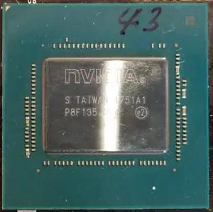
| main image |  + + |
| manufacturer | TSMC + |
| market segment | Artificial Intelligence + and Embedded + |
| max cpu count | 4 + |
| max memory bandwidth | 127.1 GiB/s (130,150.4 MiB/s, 136.473 GB/s, 136,472.586 MB/s, 0.124 TiB/s, 0.136 TB/s) + |
| max memory channels | 8 + |
| microarchitecture | Carmel + and Volta + |
| model number | Tegra194 + |
| name | Xavier + |
| process | 12 nm (0.012 μm, 1.2e-5 mm) + |
| smp max ways | 4 + |
| supported memory type | LPDDR4X-4266 + |
| tdp | 30 W (30,000 mW, 0.0402 hp, 0.03 kW) + |
| tdp (typical) | 20 W (20,000 mW, 0.0268 hp, 0.02 kW) + |
| technology | CMOS + |
| thread count | 8 + |
| transistor count | 9,000,000,000 + |
| word size | 64 bit (8 octets, 16 nibbles) + |