From WikiChip
Editing intel/cores/kaby lake g
Warning: You are not logged in. Your IP address will be publicly visible if you make any edits. If you log in or create an account, your edits will be attributed to your username, along with other benefits.
The edit can be undone.
Please check the comparison below to verify that this is what you want to do, and then save the changes below to finish undoing the edit.
This page supports semantic in-text annotations (e.g. "[[Is specified as::World Heritage Site]]") to build structured and queryable content provided by Semantic MediaWiki. For a comprehensive description on how to use annotations or the #ask parser function, please have a look at the getting started, in-text annotation, or inline queries help pages.
| Latest revision | Your text | ||
| Line 26: | Line 26: | ||
=== Graphics === | === Graphics === | ||
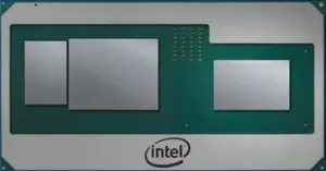
| − | Those processors are unique in the fact that this is the first time Intel has integrated a discrete graphics processor into the same package as the microprocessor. This is also the first time they are using a competitor | + | Those processors are unique in the fact that this is the first time Intel has integrated a discrete graphics processor into the same package as the microprocessor. This is also the first time they are using a competitor graphics processor. Those parts incorporate an [[AMD]] [[GPU]] based on the {{amd|Vega|l=arch}} microarchitecture and incorporate their own 4 GiB of [[high-bandwidth memory]] 2 (HBM2). The HBM solution is connected to the graphics processor using Intel's [[EMIB]], a high-speed in-package interconnect solution. |
The CPU itself is connected to the GPU using 8 of the other PCIe lanes, leaving the 8 remaining lanes for other peripherals to communicate with the CPU directly. | The CPU itself is connected to the GPU using 8 of the other PCIe lanes, leaving the 8 remaining lanes for other peripherals to communicate with the CPU directly. | ||
| Line 32: | Line 32: | ||
[[File:kaby lake g with amd radeon package.png|600px]] | [[File:kaby lake g with amd radeon package.png|600px]] | ||
| + | |||
=== Common Features === | === Common Features === | ||
Facts about "Kaby Lake G - Cores - Intel"
| designer | Intel + and AMD + |
| first announced | November 6, 2017 + |
| first launched | January 7, 2018 + |
| instance of | core + |
| isa | x86-64 + |
| isa family | x86 + |
| main image |  + + |
| main image caption | Package front + |
| manufacturer | Intel + and GlobalFoundries + |
| microarchitecture | Kaby Lake + |
| name | Kaby Lake G + |
| process | 14 nm (0.014 μm, 1.4e-5 mm) + |
| technology | CMOS + |
| word size | 64 bit (8 octets, 16 nibbles) + |