(die) |
(→Die size) |
||
| (9 intermediate revisions by the same user not shown) | |||
| Line 1: | Line 1: | ||
{{title|Die}} | {{title|Die}} | ||
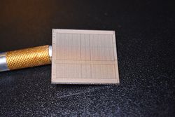
| − | A '''die''' is the actual IC chip and is the final product of the [[fabrication process]]. It is the individual chip made following the [[singulation]] of a [[wafer]]. Dies typically undergo packaging before being sold to the customer as a final product. | + | [[File:ibm power9 die.jpg|right|250px|thumb|IBM {{ibm|Power9|l=arch}} die.]] |
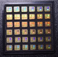
| + | [[File:6x6_waffle_pack.jpg|right|thumb|200px||A [[waffle pack]] with 36 dies.]] | ||
| + | A '''die''' is the actual bare IC chip and is the final product of the [[fabrication process]]. It is the individual chip made following the [[singulation]] of a [[wafer]]. Dies typically undergo packaging before being sold to the customer as a final product. | ||
| + | |||
| + | == Overview == | ||
| + | The die is the final product of the [[fabrication process]]. A fully processed wafer will under [[singulation]] following [[wafer probing|probing]]. Depending on the application, the die may be shipped to an assembly/packaging plant where it will undergo [[encapsulation]], producing the final chip that ships to customers. | ||
| + | |||
| + | === Known good die === | ||
| + | {{main|known good die|l1=Known Good Die (KGD)}} | ||
| + | A '''[[known good die]]''' is a special type of bare die that underwent additional testing and screening post-[[singulation]]. KGD testing ensures the die meets the required specification prior to getting packaged. KGDs are especially important in [[multi-chip packages]] where multiple dies in a single package must function correctly to produce the required product. | ||
| + | |||
| + | == Die size == | ||
| + | {{main|die size}} | ||
| + | Die size refers to the length and width of the die. Since the die size and shape determines the total number of dies that may be realized from a single [[wafer]], the die size is a strong indicator of cost. | ||
| + | |||
| + | {| class="wikitable" | ||
| + | ! colspan="4" | Select Large Dies | ||
| + | |- | ||
| + | ! GPU !! Server !! Desktop !! Mobile | ||
| + | |- style="vertical-align: top;" | ||
| + | | | ||
| + | * 826 mm² (GA100) | ||
| + | * 815 mm² (GV100) | ||
| + | * 754 mm² (TU102) | ||
| + | * 610 mm² (GP100) | ||
| + | * 601 mm² (GM200) | ||
| + | * 596 mm² (Fiji) | ||
| + | * 576 mm² (GT200) | ||
| + | * 56 mm²1 (GK110) | ||
| + | * 545 mm² (TU104) | ||
| + | * 510 mm² (Vega 10) | ||
| + | * 484 mm² (G80) | ||
| + | * 471 mm² (GP102) | ||
| + | * 445 mm² (TU106) | ||
| + | | | ||
| + | * 8x 74 mm² + 1x 416 mm² ({{amd|Rome|l=core}}) | ||
| + | * 4x 213 mm² ({{amd|Naples|l=core}}) | ||
| + | * 720 mm² ({{intel|Knights Corner|l=arch}}) | ||
| + | * 694 mm² (SKL LCC) | ||
| + | * 693 mm² ({{ibm|Power9|l=arch}}) | ||
| + | * 662 mm² (HSW HCC) | ||
| + | * 649 mm² ({{ibm|Power8|l=arch}}) | ||
| + | * 637 mm² (SPARC64 X) | ||
| + | * 600 mm² (SPARC64 X+) | ||
| + | * 567 mm² ({{ibm|Power7|l=arch}}) | ||
| + | * 513 mm² (SPARC64 VIIIfx) | ||
| + | * 492 mm² (HSW MCC) | ||
| + | * 485 mm² (SKL LCC) | ||
| + | * 456 mm² (BDW HCC) | ||
| + | * 444 mm² (SPARC64 VII) | ||
| + | * 421 mm² (SPARC64 VI) | ||
| + | * 412 mm² ({{ibm|Power4|l=arch}}) | ||
| + | * 389 mm² (Power5) | ||
| + | * 380 mm² (SPARC64 V) | ||
| + | * 362 mm² (Power8 6C) | ||
| + | * 354 mm² (HSW LCC) | ||
| + | * 341 mm² (Power6) | ||
| + | * 325 mm² (SKL LCC) | ||
| + | * 306 mm² (BDW MCC) | ||
| + | * 270 mm² (Power3) | ||
| + | * 246 mm² (BDW LCC) | ||
| + | | | ||
| + | * 2x 74 mm² + 1x 125 mm² ({{amd|Matisse|l=core}}) | ||
| + | * 213 mm² ({{amd|Pinnacle Ridge|l=core}}) | ||
| + | * 213 mm² ({{amd|Summit Ridge|l=core}}) | ||
| + | * 210 mm² ({{amd|Picasso|l=core}}) | ||
| + | * 210 mm² ({{amd|Raven Ridge|l=core}}) | ||
| + | * 199 mm² ({{intel|Comet Lake S|Comet Lake 10C|l=core}}) | ||
| + | * 174 mm² ({{intel|Comet Lake S|Coffee Lake 8C|l=core}}) | ||
| + | * 156 mm² ({{amd|Renoir|l=core}}) | ||
| + | * 150 mm² ({{intel|Comet Lake S|Coffee Lake 6C|l=core}}) | ||
| + | * 123 mm² ({{intel|Ice Lake U|Ice Lake 4C|l=core}}) | ||
| + | * 122 mm² ({{intel|Skylake S|Skylake 4C|l=core}}) | ||
| + | * 102 mm² ({{intel|Skylake U|Skylake 2C|l=core}}) | ||
| + | | | ||
| + | * 163 mm² (A5X) | ||
| + | * 147 mm² (A9X) | ||
| + | * 128 mm² (A8X) | ||
| + | * 125 mm² (A10) | ||
| + | * 123 mm² (A6X) | ||
| + | * 122 mm² (A12X) | ||
| + | * 122 mm² (A12) | ||
| + | * 122 mm² (A5) | ||
| + | * 104 mm² (A9) | ||
| + | * 102 mm² (A7) | ||
| + | * 96 mm² (A10X) | ||
| + | * 95 mm² (A6) | ||
| + | * 89 mm² (A8) | ||
| + | * 88 mm² (A11) | ||
| + | * 53 mm² (A4) | ||
| + | |} | ||
| + | {{expand list}} | ||
| + | |||
| + | == See also == | ||
| + | * [[yield]] | ||
Revision as of 02:36, 1 June 2020


A die is the actual bare IC chip and is the final product of the fabrication process. It is the individual chip made following the singulation of a wafer. Dies typically undergo packaging before being sold to the customer as a final product.
Contents
Overview
The die is the final product of the fabrication process. A fully processed wafer will under singulation following probing. Depending on the application, the die may be shipped to an assembly/packaging plant where it will undergo encapsulation, producing the final chip that ships to customers.
Known good die
- Main article: Known Good Die (KGD)
A known good die is a special type of bare die that underwent additional testing and screening post-singulation. KGD testing ensures the die meets the required specification prior to getting packaged. KGDs are especially important in multi-chip packages where multiple dies in a single package must function correctly to produce the required product.
Die size
- Main article: die size
Die size refers to the length and width of the die. Since the die size and shape determines the total number of dies that may be realized from a single wafer, the die size is a strong indicator of cost.
| Select Large Dies | |||
|---|---|---|---|
| GPU | Server | Desktop | Mobile |
|
|
|
|
This list is incomplete; you can help by expanding it.