(basic overview) |
(→Overview: +ring info) |
||
| Line 27: | Line 27: | ||
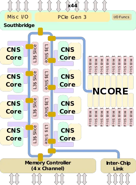
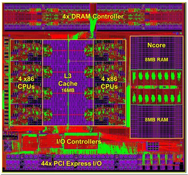
CHA is an [[x86]] SoC designed by [[Centaur]] for the server, edge, and AI market. Fabricated on TSMC [[16 nm process]], the chip integrates 8 new high-performance [[x86]] "CNS" cores [[ring interconnect|interconnected on a ring]] along with a high-performance "NCORE" [[neural processor]]. This chip is the first server x86 chip to integrate an AI accelerator right on-die and is designed to reduce the dependency on AI acceleration through additional hardware in order to simplify the platform and cost. | CHA is an [[x86]] SoC designed by [[Centaur]] for the server, edge, and AI market. Fabricated on TSMC [[16 nm process]], the chip integrates 8 new high-performance [[x86]] "CNS" cores [[ring interconnect|interconnected on a ring]] along with a high-performance "NCORE" [[neural processor]]. This chip is the first server x86 chip to integrate an AI accelerator right on-die and is designed to reduce the dependency on AI acceleration through additional hardware in order to simplify the platform and cost. | ||
| − | The CHA SoC incorporates both the [[source bridge]] and [[north bridge]] on-die. The chip supports for up to quad-channel DDR4 memory and up to 44 PCIe Gen 3 lanes. Additionally, CHA supports the ability directly link to a second CHA SoC in a 2-way multiprocessing configuration. | + | The CHA SoC incorporates both the [[source bridge]] and [[north bridge]] on-die. The chip supports for up to quad-channel [[DDR4 memory]] and up to 44 PCIe Gen 3 lanes. Additionally, CHA supports the ability to directly link to a second CHA SoC in a 2-way [[multiprocessing]] configuration. |
| + | |||
| + | === Ring === | ||
| + | CHA interlinks all the components on the chip through a bidirectional [[ring interconnect]]. There is a dedicated ring stop for every one of the eight CNS cores connected at the [[L3 cache]] slice, one for the NCORE [[neural processor|NPU]], one for the [[southbridge]], and another one for the [[memory controller]]. | ||
| + | |||
| + | The ring itself consists of two opposing unidirectional rings. Each ring is 512-bit wide. Each cycle, data is passed from one ring stop to the next ring stop. The ring operates at the same clock frequency as the cores. At 2.5 GHz, the ring has a peak theoretical bidirectional bandwidth of 2.56 Tb/s or 320 GB/s. | ||
== CNS Core == | == CNS Core == | ||
Revision as of 23:11, 22 January 2020
| Edit Values | |
| CHA µarch | |
| General Info | |
| Arch Type | CPU |
| Designer | Centaur Technology |
| Manufacturer | TSMC |
| Process | 16 nm |
| Core Configs | 8 |
| Instructions | |
| ISA | x86-64 |
CHA is a 16-nanometer x86 SoC microarchitecture designed by Centaur Technology for the server market.
Contents
Process technology
| This section is empty; you can help add the missing info by editing this page. |
Architecture
Key changes from CN
| This section is empty; you can help add the missing info by editing this page. |
Block Diagram
CHA SoC
CNS Core
NCORE NPU
Overview
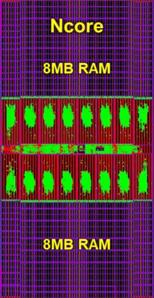
CHA is an x86 SoC designed by Centaur for the server, edge, and AI market. Fabricated on TSMC 16 nm process, the chip integrates 8 new high-performance x86 "CNS" cores interconnected on a ring along with a high-performance "NCORE" neural processor. This chip is the first server x86 chip to integrate an AI accelerator right on-die and is designed to reduce the dependency on AI acceleration through additional hardware in order to simplify the platform and cost.
The CHA SoC incorporates both the source bridge and north bridge on-die. The chip supports for up to quad-channel DDR4 memory and up to 44 PCIe Gen 3 lanes. Additionally, CHA supports the ability to directly link to a second CHA SoC in a 2-way multiprocessing configuration.
Ring
CHA interlinks all the components on the chip through a bidirectional ring interconnect. There is a dedicated ring stop for every one of the eight CNS cores connected at the L3 cache slice, one for the NCORE NPU, one for the southbridge, and another one for the memory controller.
The ring itself consists of two opposing unidirectional rings. Each ring is 512-bit wide. Each cycle, data is passed from one ring stop to the next ring stop. The ring operates at the same clock frequency as the cores. At 2.5 GHz, the ring has a peak theoretical bidirectional bandwidth of 2.56 Tb/s or 320 GB/s.
CNS Core
| This section is empty; you can help add the missing info by editing this page. |
NCORE NPU
| This section is empty; you can help add the missing info by editing this page. |
Die
SoC
- TSMC 16 nm process
- 195 mm²
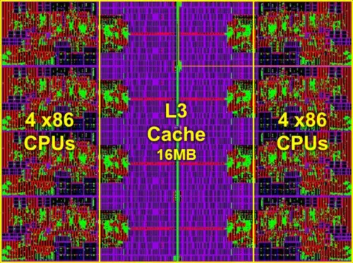
Core group
NCORE
Bibliography
- Centaur. personal communication. November 2019.
See also
- Direct Competition
| codename | CHA + |
| core count | 8 + |
| designer | Centaur Technology + |
| full page name | centaur/microarchitectures/cha + |
| instance of | microarchitecture + |
| instruction set architecture | x86-64 + |
| manufacturer | TSMC + |
| microarchitecture type | CPU + |
| name | CHA + |
| process | 16 nm (0.016 μm, 1.6e-5 mm) + |
