Semiconductor & Computer Engineering
| Line 5: | Line 5: | ||
A '''buffer''', is a basic [[logic gate]] that passes its input, unchanged, to its output. It's behavior is the opposite of a [[NOT gate]]. The main purpose of a buffer is to regenerate the input, usually using a strong high and a strong low. A buffer has one input and one output; its input always equals its input. Buffers are also used to increase the propagation delay of circuits by driving the large capacitive loads. | A '''buffer''', is a basic [[logic gate]] that passes its input, unchanged, to its output. It's behavior is the opposite of a [[NOT gate]]. The main purpose of a buffer is to regenerate the input, usually using a strong high and a strong low. A buffer has one input and one output; its input always equals its input. Buffers are also used to increase the propagation delay of circuits by driving the large capacitive loads. | ||
| − | == | + | == Description == |
| − | + | {{expand section}} | |
| + | A buffer is a very basic active device that generates an output identical to its input input. In most technologies, a buffer is made of two [[inverter]] back-to-back. One of the many purposes for a buffer is to generate weak output from [[non-restoring logic]] that was used. | ||
| + | ==Design== | ||
| + | {{empty section}} | ||
| + | |||
| + | == Symbolic representation == | ||
| + | Buffers are typically drown on schematics using one of a standard symbol. Below are three of the commonly found standard symbols. | ||
{| class="wikitable" | {| class="wikitable" | ||
|- | |- | ||
| − | ! ANSI !! IEC !! DIN | + | ! ANSI !! IEC !! DIN !! British |
|- | |- | ||
| − | | [[File: | + | | [[File:buffer gate (ansi).svg|100px]] || [[File:buffer gate (iec).svg|100px]] || [[File:buffer gate (din).svg|100px]] || [[File:buffer gate (british).svg|100px]] |
|} | |} | ||
| − | == CMOS | + | ==Implementations== |
| + | A buffer can be implemented in variety of of technologies. | ||
| + | |||
| + | === CMOS === | ||
A CMOS buffer gate with one input and one output can be realized as simply two [[inverter]]s back to back - built out of just 4 gates. | A CMOS buffer gate with one input and one output can be realized as simply two [[inverter]]s back to back - built out of just 4 gates. | ||
| Line 31: | Line 40: | ||
[[File:Buffer gate cmos.png|200px]] | [[File:Buffer gate cmos.png|200px]] | ||
{{clear}} | {{clear}} | ||
| − | == Discrete chips == | + | == Discrete Chips == |
| + | Various buffers/drivers exist chips as well for both [[7400 series]] and [[4000 series]]. | ||
| + | |||
| + | === [[7400 series]] chips === | ||
| + | {{empty section}} | ||
| + | |||
| + | === [[4000 series]] chips === | ||
| + | {{empty section}} | ||
| + | |||
The 7407 is a TTL chip with 14 pins. Two pins are used for V<sub>DD</sub> and GND, the other 12 pins are used for the 6 independent buffers. The 4050 is a CMOS Hex Buffer with 16 pins. Two pins are used for V<sub>DD</sub> and GND, 12 pins are used for the 6 independent buffers. Pins 13 and 16 are not connected. Both chips implement the expression Q<sub>N</sub> = A<sub>N</sub> | The 7407 is a TTL chip with 14 pins. Two pins are used for V<sub>DD</sub> and GND, the other 12 pins are used for the 6 independent buffers. The 4050 is a CMOS Hex Buffer with 16 pins. Two pins are used for V<sub>DD</sub> and GND, 12 pins are used for the 6 independent buffers. Pins 13 and 16 are not connected. Both chips implement the expression Q<sub>N</sub> = A<sub>N</sub> | ||
Revision as of 23:47, 15 December 2015
| Buffer Gate | ||||||||||||||||||
| ANSI Symbol | ||||||||||||||||||
.svg) | ||||||||||||||||||
| Functional | ||||||||||||||||||
 | ||||||||||||||||||
| Truth Table | ||||||||||||||||||
| ||||||||||||||||||
| ||||||||||||||||||
|
A buffer, is a basic logic gate that passes its input, unchanged, to its output. It's behavior is the opposite of a NOT gate. The main purpose of a buffer is to regenerate the input, usually using a strong high and a strong low. A buffer has one input and one output; its input always equals its input. Buffers are also used to increase the propagation delay of circuits by driving the large capacitive loads.
Contents
Description
| This section requires expansion; you can help adding the missing info. |
A buffer is a very basic active device that generates an output identical to its input input. In most technologies, a buffer is made of two inverter back-to-back. One of the many purposes for a buffer is to generate weak output from non-restoring logic that was used.
Design
| This section is empty; you can help add the missing info by editing this page. |
Symbolic representation
Buffers are typically drown on schematics using one of a standard symbol. Below are three of the commonly found standard symbols.
| ANSI | IEC | DIN | British |
|---|---|---|---|
| |
|
.svg) |
.svg)
|
Implementations
A buffer can be implemented in variety of of technologies.
CMOS
A CMOS buffer gate with one input and one output can be realized as simply two inverters back to back - built out of just 4 gates.
The table on the right shows the states of the four transistors with the various inputs of A.
| Buffer Gate by Transistor | |||||
|---|---|---|---|---|---|
| A | Q1 | Q2 | Q3 | Q4 | Q |
| 0 | 1 | 0 | 0 | 1 | 0 |
| 1 | 0 | 1 | 1 | 0 | 1 |

Discrete Chips
Various buffers/drivers exist chips as well for both 7400 series and 4000 series.
7400 series chips
| This section is empty; you can help add the missing info by editing this page. |
4000 series chips
| This section is empty; you can help add the missing info by editing this page. |
The 7407 is a TTL chip with 14 pins. Two pins are used for VDD and GND, the other 12 pins are used for the 6 independent buffers. The 4050 is a CMOS Hex Buffer with 16 pins. Two pins are used for VDD and GND, 12 pins are used for the 6 independent buffers. Pins 13 and 16 are not connected. Both chips implement the expression QN = AN
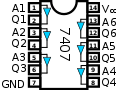
7407 Hex Buffer/Driver
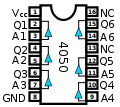
4050 CMOS Hex Buffer/Driver

