Semiconductor & Computer Engineering
| Edit Values | |
| Socket SP3 | |
| General Info | |
| Designer | AMD |
| Introduction | May 16, 2017 (announced) June 20, 2017 (launched) |
| Market | Server |
| Microarchitecture | Zen, Zen 2, Zen 3 |
| TDP | 120 W 120,000 mW , 155 W0.161 hp 0.12 kW 155,000 mW , 180 W0.208 hp 0.155 kW 180,000 mW 0.241 hp 0.18 kW |
| Package | |
| Name | SP3, FCLGA-4094 |
| Type | FC-OLGA |
| Contacts | 4094 |
| Dimension | 75.40 mm 7.54 cm × 58.50 mm2.969 in 5.85 cm × 6.26 mm2.303 in 0.246 in |
| Pitch | 0.87 mm 0.0343 in × 1.00 mm0.0394 in |
| Socket | |
| Name | SP3, LGA-4094 |
| Type | SM-LGA |
| Succession | |
| Contemporary | |
| Socket TR4 Socket sTRX4 Socket sWRX8 | |
Socket SP3 is a microprocessor socket designed by AMD for the first three generations of their EPYC family of high performance server processors. It supports eight channels of DDR4 memory and eight 16-lane PCIe I/O links. Socket SP3 succeeded Socket G34 and was superseded by Socket SP5.
Three other sockets were derived from, and are mechanically identical to Socket SP3 but differ electrically: Socket TR4 a.k.a. Socket SP3r2 for first and second generation, and Socket sTRX4 for third generation Ryzen Threadripper high end desktop processors. These infrastructures support only four memory channels and UDIMMs instead of RDIMMs. Processors for these sockets are not compatible with Socket SP3 or vice versa. Socket sWRX8 is designated for Ryzen Threadripper workstation processors which support eight memory channels and both UDIMM and RDIMM types.
For mainstream desktop processors AMD developed Socket AM4. Contemporary mobile and embedded processors use the BGA packages FT5, FP5, FP6, and SP4.
Contents
Overview[edit]
Socket SP3 is a zero insertion force, screw actuated, surface-mount land grid array socket for use with a 4094-contact, 1.00 mm × 0.87 mm interstitial pitch, organic land grid array CPU package.
It supports eight channels of 72-bit DDR4 memory with up to 2 DIMMs per channel, eight 16-lane PCIe Gen 3/4 I/O links, three or four of which are repurposed as inter-socket links on dual socket systems, four USB 3.1 Gen 1 ports, and up to 32 SATA Gen 3 ports.
This compares to four DDR3 channels and five HyperTransport links on its predecessor Socket G34, while the newer Socket SP5 supports 12 channels of DDR5 memory, eight PCIe Gen 5 links, and four USB 3.2 Gen 1 ports. (SP4 and SP4r2 are ball grid array packages of EPYC 3000 embedded processors.)
The following AMD processor families use Socket SP3:
| CPU Family | Microarch. | Process | Products | |
|---|---|---|---|---|
| Type 0 | Family 17h Models 00h–0Fh | Zen | 14 nm | EPYC 7001 "Naples" (Model 01h), EPYC Embedded 7001 |
| Type 1 | Family 17h Models 30h–3Fh | Zen 2 | 7 nm | EPYC 7002 "Rome" (Model 31h), EPYC Embedded 7002 |
| Type 2 | Family 19h Models 00h–0Fh | Zen 3 | 7 nm | EPYC 7003 "Milan" (Model 01h) |
Codenames of AMD SP3 reference platforms (CRBs) are "Diesel", "Ethanol", "Daytona", and "Ethanol-X".
Specifications of a dual socket EPYC blade motherboard and collaterals including BOM, CAD file, CPLD programming data, Eagle layout, and schematic were published by the Open Compute Project under Project Olympus AMD EPYC, specifically the US1-EPYC implementation by Quanta.
Package Description[edit]
The SP3 CPU package is lidded, has a 58.50 mm × 75.40 mm organic substrate with flip chip die attachment, 4094 nickel and gold plated land pads, and weighs up to 140 g. It leaves AMD's OSAT partner in a shipping tray with a carrier frame pre-installed. The carrier frame is a part of the package loading mechanism and remains on the package in the socket.
The package substrate has six keying notches along the short edges preventing it from being inserted 180 degrees rotated into the carrier frame or socket, or in an incompatible socket with mismatching keying features. Four additional positions are reserved for future models. However all sockets SP3, TR4, sTRX4, and sWRX8, and all processors for these sockets have the same keying. It is worth noting that these processors are also electrically keyed by pin CORETYPE, SP3R1, and SP3R2, and SP3 motherboards are not supposed to power up the socket if a TR4 or sTRX4 processor is installed. To boot the processor compatible firmware is also required. A triangular symbol on both sides of the substrate marks the location of pin A1, with corresponding markings on the socket.
The lid a.k.a. integrated heat spreader of Type-0 processors has an internal support bar bisecting their four dies. SP3 packages place decoupling capacitors under the lid around the chiplet periphery on the top side, and in two windows in the pad grid on the bottom side.
All SP3 packages are multi-chip modules. Type-0 packages integrate four identical "Zeppelin" rev. ZP-B2 dies, each containing eight CPU cores and implementing one quarter of the processor's memory and I/O interfaces. AMD used the same dies in various revisions for first generation EPYC server and embedded processors, and the first two generations of Ryzen Threadripper and Ryzen desktop processors without iGPU; see CPU Family 17h. Customized, single-ended, 4:1 SerDes links routed on two package layers, 32 lanes wide in each direction, connect the dies. AMD chose not to route these signals on a 2.5D interposer or EMIB for reasons of product flexibility and reach. The SerDes run at FCLK so for instance a 1.33 GHz FCLK coupled to the bus clock of DDR4-2666 SDRAM gives a raw data rate of 5.33 GT/s per lane or 21.33 GB/s in each direction. The following diagram illustrates the routing of high speed signals between the dies and the package contacts. Four package layers were used for these signals: Layer A, B, or both for the GMI links, C & D for the xGMI and I/O links, and all four layers (one per channel) for the memory interfaces.

Type-1/2 packages integrate one central I/O die and 2, 4, 6, or 8 identical Core Complex Dies which contain eight CPU cores each, populated in order CCD2/CCD4, CCD0/CCD6, and CCD1/CCD7. This silicon is "Starship" rev. SSP-B0 (CPU Family 17h) and "Genesis" GN-B1 (19h). AMD used the same chips, possibly different revisions, for second and third generation EPYC server and embedded processors, and Ryzen Threadripper HEDT and workstation processors.

Socket SP3 supports eight 72-bit DDR4 memory channels A-H with up to 2 DIMMs per channel. The DIMMs are placed in order A-D and E-H parallel to the socket's broad sides. This also applies to Socket sTRX4 (where only the four channels A, D, E, and H are available), Socket sWRX8 (with a maximum of one DIMM per channel), as well as SP3 and sTRX4 motherboards supporting only one DIMM per channel as a trade-off between performance (as point-to-point connections improve signal integrity and permit higher data rates), board size and memory capacity.
Furthermore Socket SP3 supports eight 16-lane multi-function I/O interfaces P0-P3 and G0-G3. All of these interfaces can be configured as PCIe link, some alternatively as xGMI link or S-Link, and some lanes as SATA, SATA Express, or XGBE link.
S-Link is a cache coherent link to CCIX memory expanders introduced on Type-1 processors. As AMD switched to CXL, first available on Socket SP5, support for S-Link and CCIX/PCIe ESM mode (using 25 GT/s PHYs on Type-1/2 IODs) was canceled.
SATA Express combines PCIe and SATA controllers on the same two lanes with a GPIO pin for a device to indicate its controller type. XGBE links support the 10GBASE-KR, 1000BASE-KX, and SGMII (10/100/1000 Mbit/s) backplane Ethernet protocols. The SATAe and XGBE functions are implemented on Type-0 processors but not Type-1/2, and support for these interfaces on Socket SP3 was withdrawn.

On dual socket (2P) systems the cache coherent xGMI links connect the Data Fabrics of each processor. Type-0 processors use four links, each attached to one die on the package, creating a NUMA system with three memory distances and one or two hops between any two dies. Type-1/2 processors can use three or four xGMI links depending on bandwidth requirements, all connected to the central I/O die. xGMI links use 16 lanes, unused links release 16 lanes per socket for I/O. The integrated SMU dynamically adjusts the link width (number of active lanes) for power saving. The WAFL link, one or two lanes, connect the Control Fabrics on each processor, i.e. the PSP, SMUs and other IPs, primarily for temperature monitoring, power and frequency control. Four socket systems are not supported although the available resources do not seem to rule this out.
Type-0 processors support DDR4-2666 memory and PCIe Gen 3 (8 GT/s) on their I/O links. Type-1/2 processors support DDR4-3200 memory and PCIe Gen 4 (16 GT/s), with xGMI links reaching 18 GT/s. Optimized motherboards are required to realize these data rates. Accordingly Type-1 processors can only run at restricted rates on Type-0 boards, after a BIOS update providing compatible firmware. Type-2 processors are not supported on first generation EPYC boards. Conversely EPYC 7001 "Naples" processors are incompatible with dual socket boards implementing only three xGMI links.
Socket Description[edit]
Socket SP3, TR4, sTRX4, and sWRX8 are mechanically identical. They have a 79.9 mm × 120.3 mm footprint and consist of the following components, from top to bottom:
- Force Frame
- Rail Frame
- Socket Housing
- Stiffener Frame
- Insulators
- Backplate
Removable components are:
- Heatsink
- Carrier Frame
- External Cap
- PnP Cover Cap
The force frame, rail frame, and stiffener frame constitute the Socket Actuation Mechanism. The heatsink, the CPU in a carrier frame, the SAM, housing, and backplate are separately orderable parts. The latter three are motherboard components for OEMs. Socket SP3 suppliers are Foxconn Interconnect Technology (website) and Lotes Co. Ltd. (website).
LGA sockets use cantilever springs in the socket housing to make electrical contact with flat pads on the bottom of the CPU package. The SAM creates the Z-axis compression load between the CPU package and the housing soldered to the motherboard. Considerable force is required to deflect thousands of springs at once. According to AMD the SP3 SAM must exert a minimum force of 95 kg-f (932 N) to ensure proper mating of the package with the socket, a maximum of 125 kg-f (1226 N), so SP3 sockets are not actuated by a lever but three Torx screws linking their force frame and stiffener frame. The stiffener frame is attached to the backplate on the bottom side of the motherboard.
The force frame a.k.a. load plate is a largely flat piece stamped out of 2.0 mm thick stainless steel sheets. It has a window allowing the top of the CPU package lid to protrude for contact with the heatsink. When actuated it applies a load to the flanges on the sides of the lid. The force frame is attached to the stiffener frame by a hinge. It permits vertical motion when the socket is actuated, integrates a torsional spring to keep the frame open while the user inserts or removes the CPU, and a stop feature limiting the opening angle to some 105 degrees. The force frame is actuated by three captive screws with a Torx T20 head and M3.5×0.6 or larger thread. They mate with self-clinching PEM nuts on the stiffener frame.
These screws must be tightened in a particular order to avoid damage to the contact springs, the order is marked on the force frame. The lone screw opposite the hinge first, followed by the two screws next to it, with a maximum torque of 16.1 ± 1.2 kgf-cm (14.0 ± 1.0 lbf-in, 1.58 ± 0.1 N⋅m) according to AMD. Ryzen Threadripper boxed processors come with a small preset torque limiting screwdriver for this purpose. Some sources recommend two passes to engage the threads, then tighten the screws. To remove the processor the screws should be opened in reverse order.
The rail frame together with the carrier frame constitute the package loading mechanism. Its main purpose is to minimize the risk of contact spring damage due to handling errors or accidents when loading the package into the housing. The rail frame is a stainless steel frame overmolded with black polycarbonate plastic and attached to the stiffener frame with a second hinge similar to the force frame. The steel frame forms a closed loop for stability and extends into a pair of finger lift tabs marked with blue color. The carrier frame slides into the rail frame along rails molded into both parts. They also have locking features which secure the carrier frame in the final position. When the rail frame is closed, latching features engage with undercut steps on the housing to ensure the package remains properly seated during actuation.
The carrier frame is made from colored polycarbonate material. EPYC 7001 series processors use blue, 7002 series green, 7003 series grey, and Threadripper processors (for Socket TR4, sTRX4, and sWRX8) orange carriers. The carrier frame has a window for the package lid and a handle to pick up, insert, and remove the carrier without touching and contaminating the contact pads on the package. The handle bears the name of the supplier, commonly Lotes, and has a hole to provide access for one of the actuation screws. The opposite side of the frame is marked with a date and revision code. The carrier frame has six latches and is designed to snap onto the top side of the package substrate while the CPU package is sitting in the shipping tray. Keying features match two keying notches in the package to prevent it from being inserted 180 degrees rotated. Four alignment pegs on the carrier frame engage with alignment holes in the socket housing when the rail frame is closed.
The carrier frame is not supposed to be removed and not sold to consumers. Owners of a processor under warranty with a broken frame should contact the vendor or AMD customer service. Third parties may sell carrier frames salvaged from defective CPUs. If a replacement can or should be 3D-printed is unclear. It is evidently possible, with some care, to insert the package into the housing without the carrier.
The external cap is made from a transparent polycarbonate material. It has the same outer dimensions as the carrier frame, and the same rail and locking features to slide into the rail frame. The external cap ships with the SAM and protects the contact springs when no processor is installed in the socket. A label on its top side reminds users to remove the cap before inserting the processor. On the reverse side the external cap has a cavity fitting the cover cap, so the SAM with external cap can be installed over the housing with cover cap.
The cover cap is made from black liquid crystal polymer (LCP). It has the same alignment pegs as the carrier frame and latching features engaging with undercut steps on the housing, separate from those for the rail frame. The position of the pegs is asymmetric so the cap cannot be installed 180 degrees rotated. The cover cap ships with the socket housing and facilitates pick-and-place with a vacuum nozzle during board assembly. Its top protrusion has vent holes, bears the name of the socket and supplier, and serves as an alignment feature against the SAM with external cap.
The socket housing is a black LCP casing with two windows where decoupling capacitors can be placed on the top side of the motherboard. Its outline is asymmetric, preventing the SAM from being installed 180 degrees rotated. The walls have undercut steps on the outside for the rail frame and cover cap latches, cavities accomodating the carrier frame latches and keying features, finger access cut-outs in the middle of the long edges, and four alignment holes to receive the alignment pegs on the carrier frame. A chamfered corner marks the location of pin A1. The contact springs extend into a J-lead at the bottom of the housing with 0.6 mm diameter solder balls attached for surface mounting. Standoffs limit the distance to the PCB.
The stiffener frame a.k.a. base plate is a flat, 1.7 mm thick stainless steel plate with a window fitting the socket housing, and seven self-clinching, flush integrated nuts to fasten the force frame and a heatsink. The position of the four heatsink nuts (PEM nut standoffs) is asymmetric so the heatsink can only be installed in one orientation. They have a M3.5×0.6 internal thread, and height 6.0 mm including the stiffener frame thickness or 6.18 mm from the top of the PCB. The top of the CPU package lid is 8.959 mm from the top of the PCB when the socket is actuated.
The SAM must be attached to a backplate on the bottom side of the motherboard or directly mounted to the chassis. This is facilitated by four M3.5×0.6 captive nuts on the stiffener frame with a Torx T20 head, a head diameter of 6.0 mm and maximum head height of 2.3 mm, to be tightened in a diagonal pattern with a maximum torque of 16.1 ± 1.2 kgf-cm (14.0 ± 1.0 lbf-in, 1.58 ± 0.1 N⋅m).
The backplate is a flat, 2.5 mm thick stainless steel plate with four self-clinching studs with a M3.5×0.6 external thread. Its dimensions are symmetric so it can be installed 180 degrees rotated, and like the housing it has a window for bottom side components. The studs protrude upwards through holes in the PCB and mate with the captive nuts on the stiffener frame. Backplates with stud heights between 4.0 and 5.6 mm are available to account for different PCB thicknesses.
Two sheets made from insulating material, 0.18 mm thick and about as large as the respective metal part separate the stiffener frame and backplate from the motherboard.
Socket SP3 processors require a heatsink. Heatsinks weighing up to 450 g can be mounted to the PEM nuts on the stiffener frame, heavier heatsinks require additional support such as direct chassis attachment. The allowable spring force exerted by the heatsink on the package lid is 75 ± 15 lb-f (334 ± 67 N). Thermal interface material should be applied between the lid and heatsink. The four captive spring screws on the heatsink should be tightened in a diagonal pattern with the same maximum torque of 16.1 ± 1.2 kgf-cm (14.0 ± 1.0 lbf-in, 1.58 ± 0.1 N⋅m) as the actuation screws.
Feature Summary[edit]
- Lidded land grid array package, 75.40 mm × 58.50 mm
- 4094 contacts in a 82 × 55 grid with 0.87 mm × 1.00 mm interstitial pitch
- Organic substrate, flip chip die attachment
- 8 × 72 bit DDR4 SDRAM interface
- Type-0 processors: Up to 1333 MHz, PC4-21333 (DDR4-2666), 170.67 GB/s total raw bandwidth
- Type-1/2 processors: Up to 1600 MHz, PC4-25600 (DDR4-3200), 204.8 GB/s total raw bandwidth
- Up to 2 DIMMs/channel, up to 16 DIMMs total
- RDIMM, LRDIMM, 3DS DIMM, NVDIMM-N types
- ECC supported
- Memory capacity 256 GiB/channel (Type-0) or 512 GiB/channel (Type-1/2)
- Eight multi-function I/O interfaces P0-P3, G0-G3
Lane 15 14 13 12 11 10 9 8 7 6 5 4 3 2 1 0 xGMI S-Link PCIe x16 x8 x8 x4 x4 x4 x4 x2 x2 x2 x2 x2 x2 x2 x2 x1 x1 x1 x1 x1 x1 x1 x1 x1 x1 x1 x1 x1 x1 x1 x1 SATAe 1 0 SATA 7 6 5 4 3 2 1 0 XGBE 3 2 1 0 Type-0 PHYs PHY 4 PHY 3 PHY 2 PHY 1 PHY 0 Type-1/2 PHYs PHY 3 PHY 2 PHY 1 PHY 0
- PCIe protocol supported on all interfaces
- Type-0 processors: PCIe Gen 1, 2, 3 (8 GT/s)
- Type-1/2 processors: PCIe Gen 1, 2, 3, 4 (16 GT/s)
- 16 lanes, up to 8 ports per interface configurable x16, x8, x4, x2, x1 with power-of-two alignment (e.g. 1x4 + 4x1 + 1x8)
- Max. 7 PCIe ports in each 8-lane subset (e.g. 0x8 + 8x1 is not possible)
- Max. 7 PCIe ports per interface if any lane is configured as SATA port
- Different PCIe generations supported on the ports in the same interface
- Lane polarity inversion, per port lane reversal
- Up to 128 PCIe lanes total on 1P systems
- Up to 64 or 80 PCIe lanes total per socket on 2P systems
- PCIe protocol supported on all interfaces
- xGMI protocol supported on G0-G3, used on 2P systems only
- Type-0 processors: Four x16 links per socket required
- Type-1/2: Three or four links depending on bandwidth requirements
- Four links: G0 (socket 0) ↔ G2 (socket 1), G1 ↔ G3, G2 ↔ G0, G3 ↔ G1
- Three links: G0 ↔ G2, G1 ↔ G3, G2 ↔ G0
- Max. raw data rate 18 GT/s (Type-1/2)
- xGMI protocol supported on G0-G3, used on 2P systems only
- S-Link protocol on P0-P3
- Not supported on Socket SP3
- S-Link protocol on P0-P3
- SATA Gen 1, 2, 3 (6 Gb/s) protocol supported on the lower 8 lanes of P0, P1, G2, G3
- P0: SATA00-07, P1: SATA10-17, G2: SATA20-27, G3: SATA30-37
- Up to 32 SATA ports total on 1P systems
- Up to 16 SATA ports total per socket on 2P systems
- SATA Gen 1, 2, 3 (6 Gb/s) protocol supported on the lower 8 lanes of P0, P1, G2, G3
- XGBE protocols on lanes 4-7 of P0, P1, G2, G3
- P0: XGBE00-03, P1: XGBE10-13, G2: XGBE20-23, G3: XGBE30-33
- Not supported on Socket SP3
- XGBE protocols on lanes 4-7 of P0, P1, G2, G3
- Five (Type-0 processors) or four (Type-1/2) PHY groups on each interface
- Lanes sharing a PHY group must use the same protocol (PCIe, SATA)
- On Type-0 platforms lanes 0-3 must use the same protocol for compatibility with Type-1 processors
- Five (Type-0 processors) or four (Type-1/2) PHY groups on each interface
- Supplementary I/O interface
- PCIe Gen 1, 2 (5 GT/s), 2 lanes
- WAFL interface on 2P systems
- Option 1: WAFL[0] (socket 0) ↔ WAFL[1] (socket 1), WAFL[1] (s0) ↔ WAFL[0] (s1)
- Option 2 (Type-1/2 only): WAFL[0] (s0) ↔ WAFL[1] (s1), WAFL[1] (s0) and WAFL[0] (s1) not used
- Type-0 processors: Unused lanes remain unconnected
- Type-1/2: Unused lanes are available for I/O, e.g. to attach a BMC
- 4 × USB 1.1, 2.0, 3.1 Gen 1 (5 Gb/s) ports
- Low speed interfaces (some sharing pins):
Processors using Socket SP3[edit]
Photos[edit]
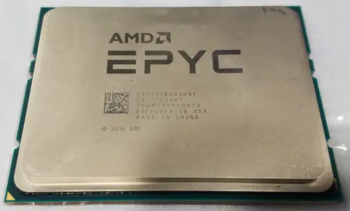
FCLGA-4094, package front

FCLGA-4094, package back

Socket SP3, open
.png)
.png)

Package Diagrams[edit]

SP3 package. All dimensions in millimeters.
 "Naples" package |
 "Rome" package |

SP3 carrier frame (AMD ref. design, not Lotes). All dimensions in millimeters.
Socket Diagrams[edit]

Socket SP3 housing (AMD). The 4094 contact springs are not shown. All dimensions in millimeters.
Foxconn version.

Socket SP3 PCB layout. NPTH = Non-Plated Through Hole. All dimensions in millimeters.
Pin Map[edit]

Socket SP3 pinout, top view. This is a preview, click for a larger image and other views.
Pin Description[edit]
Socket SP3, sTRX4, and sWRX8 have the same pinout with some constraints as noted.
| Signal | Type | Description | ||||||||||||||||
|---|---|---|---|---|---|---|---|---|---|---|---|---|---|---|---|---|---|---|
| MA-MD_ACT_L | O-IOMEM_ABCD-S | DRAM Channel A-D[1] Activation Command | ||||||||||||||||
| MA-MD_ADD[13:0] | O-IOMEM_ABCD-S | DRAM Column/Row Address | ||||||||||||||||
| MA-MD_ADD_17 | O-IOMEM_ABCD-S | DRAM Column/Row Address 17 | ||||||||||||||||
| MA-MD_ALERT_L | I-IOMEM_ABCD-S | DRAM Alert (CRC error and Command/Address parity error) | ||||||||||||||||
| MA-MD_BANK[1:0] | O-IOMEM_ABCD-S | DRAM Bank Address | ||||||||||||||||
| MA-MD_BG[1:0] | O-IOMEM_ABCD-S | DRAM Bank Group | ||||||||||||||||
| MA-MD_CAS_L_ADD[15] | O-IOMEM_ABCD-S | DRAM Column Address Strobe or Column/Row Address 15 | ||||||||||||||||
| MA-MD_CHECK[7:0] | B-IOMEM_ABCD-S | DRAM ECC Check Bits | ||||||||||||||||
| MA-MD_C[2:0] | O-IOMEM_ABCD-S | DRAM Chip ID Signals | ||||||||||||||||
| MA-MD_DATA[63:0] | B-IOMEM_ABCD-S | DRAM Data Bus | ||||||||||||||||
| MA-MD_DQS_H/L[8:0] | B-IOMEM_ABCD-S | DRAM Differential Data Strobe | ||||||||||||||||
| MA-MD_DQS_H[17:9] | B-IOMEM_ABCD-S | DRAM Differential Data Strobe for RDIMMs, DM[8:0] Data Mask output for UDIMMs[2] | ||||||||||||||||
| MA-MD_DQS_L[17:9] | B-IOMEM_ABCD-S | DRAM Differential Data Strobe for RDIMMs, not connected for UDIMMs | ||||||||||||||||
| MA-MD_EVENT_L | I-IOMEM_ABCD-S | DRAM Thermal Event | ||||||||||||||||
| MA-MD_PAROUT | O-IOMEM_ABCD-S | DRAM Command and Address Parity | ||||||||||||||||
| MA-MD_RAS_L_ADD[16] | O-IOMEM_ABCD-S | DRAM Row Address Strobe or Column/Row Address 16 | ||||||||||||||||
| MA-MD_RESET_L | O-IOMEM_ABCD-S | DRAM Reset | ||||||||||||||||
| MA-MD_WE_L_ADD[14] | O-IOMEM_ABCD-S | DRAM Write Enable or Column/Row Address 14 | ||||||||||||||||
| MA-MD_ZVSS | A | DRAM Interface Drive-Strength Auto-Compensation Resistor to VSS | ||||||||||||||||
| MA0-MD0_CKE[1:0] MA1-MD1_CKE[1:0] |
O-IOMEM_ABCD-S | DRAM Channel A-D DIMM 0-1 Clock Enable | ||||||||||||||||
| MA0-MD0_CLK_H/L[1:0] MA1-MD1_CLK_H/L[1:0] |
O-IOMEM_ABCD-D | DRAM Channel A-D DIMM 0-1 Differential Clock | ||||||||||||||||
| MA0-MD0_CS_L[1:0] MA1-MD1_CS_L[1:0] |
O-IOMEM_ABCD-S | DRAM Channel A-D DIMM 0-1 Chip Select | ||||||||||||||||
| MA0-MD0_ODT[1:0] MA1-MD1_ODT[1:0] |
O-IOMEM_ABCD-S | DRAM Channel A-D DIMM 0-1 Enable Pin for On Die Termination | ||||||||||||||||
| ME-MH_ACT_L | O-IOMEM_EFGH-S | DRAM Channel E-H[1] Activation Command | ||||||||||||||||
| ME-MH_ADD[13:0] | O-IOMEM_EFGH-S | DRAM Column/Row Address | ||||||||||||||||
| ME-MH_ADD_17 | O-IOMEM_EFGH-S | DRAM Column/Row Address 17 | ||||||||||||||||
| ME-MH_ALERT_L | I-IOMEM_EFGH-S | DRAM Alert (CRC error and Command/Address parity error) | ||||||||||||||||
| ME-MH_BANK[1:0] | O-IOMEM_EFGH-S | DRAM Bank Address | ||||||||||||||||
| ME-MH_BG[1:0] | O-IOMEM_EFGH-S | DRAM Bank Group | ||||||||||||||||
| ME-MH_CAS_L_ADD[15] | O-IOMEM_EFGH-S | DRAM Column Address Strobe or Column/Row Address 15 | ||||||||||||||||
| ME-MH_CHECK[7:0] | B-IOMEM_EFGH-S | DRAM ECC Check Bits | ||||||||||||||||
| ME-MH_C[2:0] | O-IOMEM_EFGH-S | DRAM Chip ID Signals | ||||||||||||||||
| ME-MH_DATA[63:0] | B-IOMEM_EFGH-S | DRAM Data Bus | ||||||||||||||||
| ME-MH_DQS_H/L[8:0] | B-IOMEM_EFGH-S | DRAM Differential Data Strobe | ||||||||||||||||
| ME-MH_DQS_H[17:9] | B-IOMEM_EFGH-S | DRAM Differential Data Strobe for RDIMMs, DM[8:0] Data Mask output for UDIMMs[2] | ||||||||||||||||
| ME-MH_DQS_L[17:9] | B-IOMEM_EFGH-S | DRAM Differential Data Strobe for RDIMMs, not connected for UDIMMs | ||||||||||||||||
| ME-MH_EVENT_L | I-IOMEM_EFGH-S | DRAM Thermal Event | ||||||||||||||||
| ME-MH_PAROUT | O-IOMEM_EFGH-S | DRAM Command and Address Parity | ||||||||||||||||
| ME-MH_RAS_L_ADD[16] | O-IOMEM_EFGH-S | DRAM Row Address Strobe or Column/Row Address 16 | ||||||||||||||||
| ME-MH_RESET_L | O-IOMEM_EFGH-S | DRAM Reset | ||||||||||||||||
| ME-MH_WE_L_ADD[14] | O-IOMEM_EFGH-S | DRAM Write Enable or Column/Row Address 14 | ||||||||||||||||
| ME-MH_ZVSS | A | DRAM Interface Drive-Strength Auto-Compensation Resistor to VSS | ||||||||||||||||
| ME0-MH0_CKE[1:0] ME1-MH1_CKE[1:0] |
O-IOMEM_EFGH-S | DRAM Channel E-H DIMM 0-1 Clock Enable | ||||||||||||||||
| ME0-MH0_CLK_H/L[1:0] ME1-MH1_CLK_H/L[1:0] |
O-IOMEM_ABCD-D | DRAM Channel E-H DIMM 0-1 Differential Clock | ||||||||||||||||
| ME0-MH0_CS_L[1:0] ME1-MH1_CS_L[1:0] |
O-IOMEM_EFGH-S | DRAM Channel E-H DIMM 0-1 Chip Select | ||||||||||||||||
| ME0-MH0_ODT[1:0] ME1-MH1_ODT[1:0] |
O-IOMEM_EFGH-S | DRAM Channel E-H DIMM 0-1 Enable Pin for On Die Termination | ||||||||||||||||
| FORCE_SELFREFRESH | I-IO18S5-S | NVDIMM Force Self-Refresh[3] | ||||||||||||||||
| NV_SAVE_L | O-IO18S5-S | NVDIMM SAVE Signal[3] | ||||||||||||||||
| P0-P3_RXP/RXN[15:0] | I-PCIE-D | PCIe Interface P0-P3[4] Receive Data Differential Pairs | ||||||||||||||||
| P0-P3_TXP/TXN[15:0] | O-PCIE-D | PCIe Transmit Data Differential Pairs | ||||||||||||||||
| P0A/P1A/P2B/P3B_ZVSS | A | PCIe Drive-Strength Auto-Compensation Resistor to VSS for P0-P3 | ||||||||||||||||
| G0-G3_RXP/RXN[15:0] | I-XGMI-D or I-PCIE-D | xGMI or PCIe Interface G0-G3[4] Receive Data Differential Pairs | ||||||||||||||||
| G0-G3_TXP/TXN[15:0] | O-XGMI-D or O-PCIE-D | xGMI or PCIe Transmit Data Differential Pairs | ||||||||||||||||
| G0B/G1B/G2A/G3A_ZVSS | A | PCIe Drive-Strength Auto-Compensation Resistor to VSS for G0-G3 | ||||||||||||||||
| PCIE_RST(0-3)_L | O-IO33S5-S | Reset signal for PCIe devices.[5] Type-0: from die 0-3, Type-1/2: from I/O die | ||||||||||||||||
| WAFL_RXP/RXN[1:0] | I-WAFL-D | WAFL[6] Receive Data Differential Pairs | ||||||||||||||||
| WAFL_TXP/TXN[1:0] | O-WAFL-D | WAFL Transmit Data Differential Pairs | ||||||||||||||||
| WAFL(0-3)_ZVSS | A | WAFL Drive-Strength Auto-Compensation Resistor to VSS; Type-0: die 0-3, Type-1/2: I/O die | ||||||||||||||||
| SATA(0-3)(0-7)_RXP/RXN | I-SATA-D | SATA Receive Data Differential Pairs (alt. func. of P0, P1, G2, and G3[4] lane 0-7) | ||||||||||||||||
| SATA(0-3)(0-7)_TXP/TXN | O-SATA-D | SATA Transmit Data Differential Pairs | ||||||||||||||||
| DEVSLP(0-1) | I-IO33S5-OD | SATA DEVSLP | ||||||||||||||||
| SGPIO(0-3)_CLK | O-IO33S5-S | SGPIO Interface 0-3[7] CLK Output; Type-0: from die 0-3, Type-1/2: from I/O die | ||||||||||||||||
| SGPIO(0-3)_DATAIN | I-IO33S5-S | Type-0: SGPIO DATA Input, Type-1/2: Reserved | ||||||||||||||||
| SGPIO(0-3)_DATAOUT | O-IO33S5-S | SGPIO DATA Output | ||||||||||||||||
| SGPIO(0-3)_LOAD | O-IO33S5-S | SGPIO LOAD Output | ||||||||||||||||
| XGBE(0-3)(0-3)_RXP/RXN | XGBE Receive Data Differential Pairs (alt. func. of P0, P1, G2, G3 lane 4-7)[8] | |||||||||||||||||
| XGBE(0-3)(0-3)_TXP/TXN | XGBE Transmit Data Differential Pairs | |||||||||||||||||
| MDIO(0-7)_SCL | MDIO Port 0-7 Clock (alt. func. of SGPIO interface) | |||||||||||||||||
| MDIO(0-7)_SDA | MDIO Data | |||||||||||||||||
| USB_0/1_HSD(0-3)P/N | B-IO33S5-D | USB Port 0-3 High Speed I/O Differential Pairs; Type-0: from die 0/1 (die 0 ports 0-1, die 1 ports 2-3), Type-1/2: from I/O die | ||||||||||||||||
| USB_0/1_SS_(0-3)RXP/RXN | I-USB_S5-D | USB Port 0-3 Super Speed Receive Differential Pairs; Type-0: from die 0/1 (die 0 ports 0-1, die 1 ports 2-3), Type-1/2: from I/O die | ||||||||||||||||
| USB_0/1_SS_(0-3)TXP/TXN | O-USB_S5-D | USB Port 0-3 Super Speed Transmit Differential Pairs | ||||||||||||||||
| USB_OC(0-3)_L | I-IO33S5-S | USB Port 0-3 Over Current signal from USB connector; Type-0: to die 0, 0, 1, 1; Type-1/2: to I/O die | ||||||||||||||||
| USB(0-3)_0/1_ZVSS | A | USB Port 0-3 Drive-Strength Auto-Compensation Resistor to VSS; Type-0: die 0/1, Type-1/2: I/O die | ||||||||||||||||
| UART(0-1)_CTS_L | I-IO33-S | UART Clear To Send Input (alt. func. of UART(2-3)_RXD) | ||||||||||||||||
| UART(0-1)_INTR | I-IO33-S | UART Interrupt Request | ||||||||||||||||
| UART(0-1)_RTS_L | O-IO33-S | UART Request To Send Output (alt. func. of UART(2-3)_TXD) | ||||||||||||||||
| UART(0-3)_RXD | I-IO33-S | UART Receive Data | ||||||||||||||||
| UART(0-3)_TXD | O-IO33-S | UART Transmit Data | ||||||||||||||||
| SPI_CLK | O-IO18-S | SPI Clock | ||||||||||||||||
| SPI_DO | B-IO18-S | SPI Data Out or Data[0] for multi-I/O SPI/eSPI device | ||||||||||||||||
| SPI_DI | B-IO18-S | SPI Data In or Data[1] | ||||||||||||||||
| SPI_WP_L | B-IO18-S | SPI Write Protect or Data[2] | ||||||||||||||||
| SPI_HOLD_L | B-IO18-S | SPI Hold Signal (asserted low to hold the SPI transaction) or Data[3] | ||||||||||||||||
| PSP_ROM_CS_L SPI_TPM_CS_L |
O-IO18-S | SPI Chip Select for PSP ROM or TPM | ||||||||||||||||
| SPI_CS1/CS2_L | O-IO18-S | SPI Chip Select | ||||||||||||||||
| ESPI_CLK | O-IO18-S | ESPI Clock (alt. func. of SPI_CLK) | ||||||||||||||||
| ESPI_DAT(0-3) | B-IO33-S | ESPI Data[0], Data[1:0], Data[3:0] (alt. func. of SPI_DO/DI/WP_L/HOLD_L) | ||||||||||||||||
| ESPI_CS_L | O-IO18-S | ESPI Chip Select (SPI_CS2_L) | ||||||||||||||||
| ESPI_ALERT_L | I-IO18-S | ESPI Alert Input (LDRQ0_L); Requests service from eSPI master | ||||||||||||||||
| ESPI_RESET_L | I-IO33-S | ESPI Reset Input (KBRST_L); PCIE_RST0_L suggested as reset output | ||||||||||||||||
| LPC | ROM, | 1=SPI ROM (default) | ||||||||||||||||
| LAD(0-3) | B-IO33-S | LPC Command/Address/Data | ||||||||||||||||
| LDRQ0_L | I-IO33-S | Encoded DMA/Bus Master Request 0 | ||||||||||||||||
| LFRAME_L | O-IO33-S | LPC Bus Frame | ||||||||||||||||
| LPCCLK(0-1) | O-IO33-S | LPC 33 MHz Clock | ||||||||||||||||
| LPC_CLKRUN_L | B-IO33-OD | LPC Clock Run Signal | ||||||||||||||||
| LPC_PD_L | O-IO33S5-S | LPC Power Down | ||||||||||||||||
| LPC_PME_L | I-IO33S5-S | LPC Power Management Event | ||||||||||||||||
| LPC_RST_L | O-IO33S5-S | LPC Reset | ||||||||||||||||
| LPC_SMI_L | I-IO33-S | LPC System Management Interrupt | ||||||||||||||||
| SERIRQ | B-IO33-S | Serial IRQ for DMA | ||||||||||||||||
| EMMC_CLK | eMMC Clock Output (0-200 MHz) | |||||||||||||||||
| EMMC_CMD | eMMC Command/Response (LPC_PD_L) | |||||||||||||||||
| EMMC_DAT(0-7) | eMMC Data (alt. func. of LAD0-LAD3, LPCCLK0, LPC_CLKRUN_L, LPCCLK1, SERIRQ) | |||||||||||||||||
| EMMC_DS | eMMC HS400 Data Strobe Input (LFRAME_L) | |||||||||||||||||
| EMMC_PWR_CTRL | (LPC_PME_L) | |||||||||||||||||
| I2C(0-5)_SCL | B-DUAL-OD | I2C Port 0-5 Clock | ||||||||||||||||
| I2C(0-5)_SDA | B-DUAL-OD | I2C Data | ||||||||||||||||
| SCL0 | B-IO33-OD | SMBus Port 0 Clock (alt. func. of I2C2) | ||||||||||||||||
| SDA0 | B-IO33-OD | SMBus Port 0 Data | ||||||||||||||||
| SCL1 | B-IO33S5-OD | SMBus Port 1 Clock (alt. func. of I2C3) | ||||||||||||||||
| SDA1 | B-IO33S5-OD | SMBus Port 1 Data | ||||||||||||||||
| HP_SCL, HP_SDA | Hotplug SMBus (I2C0) | |||||||||||||||||
| SFP_SCL, SFP_SDA | SFP Bus (I2C1) | |||||||||||||||||
| SPD_SCL, SPD_SDA | SPD Bus (I2C2) | |||||||||||||||||
| BMC_SCL, BMC_SDA | BMC SMBus (I2C3) | |||||||||||||||||
| AGPIO*_(0-3) | Advanced GPIO pin for interrupt, wake, or I/O; Type-0: die 0-3, Type-1/2: I/O die | |||||||||||||||||
| EGPIO*_(0-3) | Enhanced GPIO for I/O only; Type-0: die 0-3, Type-1/2: I/O die | |||||||||||||||||
| EGPIO* | Enhanced GPIO for I/O only; Type-0: die 0, Type-1/2: I/O die | |||||||||||||||||
| REFCLK100SSC_P/N | O-CLK-D or I-CLK-D | 100 MHz CPU Reference Clock; Output from BSP, or input for AP; SSC option | ||||||||||||||||
| GPP_CLK(0-3)BP/N | O-CLK-D | 100 MHz Differential PCIe Reference Clock; Type-0: from die 0-3, Type-1/2: from I/O die | ||||||||||||||||
| GPP_CLK(0-3)TP/N | O-CLK-D | 100 MHz Differential PCIe Reference Clock; Type-0: from die 0-3, Type-1/2: from I/O die | ||||||||||||||||
| X156M_H/L[3:0] | I-XGBECLK-D | Differential 156.25 MHz Reference CLK Input[8]; Type-0: to die 0-3, Type-1/2: to I/O die | ||||||||||||||||
| X32K_X1/X2 | I-IO18S5-S | 32768 Hz Clock XTAL or (X32K_X1 only) Clock Input, for the integrated RTC | ||||||||||||||||
| X48M_X1/X2 | I-IO18S5-S | 48 MHz Clock XTAL or (X48M_X1 only) Clock Input, for the integrated clock generator | ||||||||||||||||
| RTCCLK | O-IO18S5-S | 32 kHz Real Time Clock Output, e.g. BSP to AP, or for a device requiring an RTC clock | ||||||||||||||||
| KBRST_L | I-IO33-S | Keyboard Controller Reset Input (warm reset) | ||||||||||||||||
| PM_INTR_L | I-IO33-S | PM_INTR_L function for NVMe drive I2C subsystem and PCIe hot-plug subsystem | ||||||||||||||||
| PWR_BTN_L | I-IO33S5 | Power Button; Requests sleep state or causes wake event | ||||||||||||||||
| PWR_GOOD | I-IO33S5-S | Power Good Input; Asserted when all voltages and clock inputs are within specification; From motherboard to BSP, or from BSP to AP | ||||||||||||||||
| PWRGD_OUT | O-IO33S5-S | Power Good Output, from BSP to PWR_GOOD input of AP | ||||||||||||||||
| PWROK | B-IO18-OD | Power OK; Asserted by the processor after all power planes are active, the system clock generators are powered up and run stably | ||||||||||||||||
| RESET_L | B-IO18-OD | Bidirectional signal that resets the processor when asserted; Normally controlled by an internal state machine but can also be asserted by a second external source | ||||||||||||||||
| RSMRST_L | I-IO18S5-S | Resume Reset from motherboard, resets all in-processor S5 and S0 logic; Asserted on power up, deasserted when S5 power supplies are within specification | ||||||||||||||||
| SLP_S3/S5_L | O-IO33S5-S | S3/S5 Sleep State Power Plane Control Signals
| ||||||||||||||||
| SYS_RESET_L | I-IO33S5-S | System Reset Input (reset button) | ||||||||||||||||
| WAKE_L | B-IO33S5-S | PCIe WAKE_L signal, wake system out of sleep state | ||||||||||||||||
| WOL(0-3) | I_IO33S5-OD | Wake-on-LAN function | ||||||||||||||||
| NMI_SYNC_FLOOD_L | I-IO33-S | This pin signals a NMI or Sync Flood[9] | ||||||||||||||||
| ALERT_L | O-IO33-OD | Programmable pin that can indicate different events, including a SB-TSI interrupt | ||||||||||||||||
| PROCHOT_L | I-IO33-OD | Asserted to force the processor into HTC-active state | ||||||||||||||||
| SIC | I-DUAL-OD | Sideband Interface Clock[10] | ||||||||||||||||
| SID | B-DUAL-OD | Sideband Interface Data | ||||||||||||||||
| THERMTRIP_L | B-IO33-OD | Temperature Trip Input/Output | ||||||||||||||||
| BP(0-5) | B-IO18-S | Break Point Indicator; Used to trigger external test equipment such as oscilloscopes and logic analyzers | ||||||||||||||||
| DBREQ_L | I-IO18S5-S | Debug Request input to JTAG controller | ||||||||||||||||
| TCK | I-IO18S5-S | JTAG Clock | ||||||||||||||||
| TDI | I-IO18S5-S | JTAG Data Input | ||||||||||||||||
| TDO | O-IO18S5-S | JTAG Data Output | ||||||||||||||||
| TMS | I-IO18S5-S | JTAG Mode Select | ||||||||||||||||
| TRST_L | I-IO18S5-S | JTAG Reset | ||||||||||||||||
| TEST* | Test Pins | |||||||||||||||||
| XTRIG_L[7:4] | B-IO18-OD | XTRIG Debug Signals | ||||||||||||||||
| SVC_CPU, SVC_SOC | O-IO18-S | Serial VID Interface Clock for VDDCR_CPU, VDDCR_SOC regulator | ||||||||||||||||
| SVD_CPU, SVD_SOC | B-IO18-S | Serial VID Interface Data | ||||||||||||||||
| SVT_CPU, SVT_SOC | I-IO18-S | Serial VID Interface Telemetry | ||||||||||||||||
| VDDBT_RTC_G | S | Integrated Real Time Clock battery power supply, 1.5 V ±5% or 1.8 V ±5%[11] | ||||||||||||||||
| VDDCR_CPU | S | Supply voltage for the CPU core | ||||||||||||||||
| VDDCR_CPU_SENSE | A | VDDCR_CPU voltage sense output, differential feedback with VSS_SENSE_A | ||||||||||||||||
| VDDCR_SOC | S | Supply voltage for the Northbridge (integrated FCH, Ethernet, SATA, NBIO, SMU, DDR PHY logic) | ||||||||||||||||
| VDDCR_SOC_SENSE | A | VDDCR_SOC voltage sense output, differential feedback with VSS_SENSE_B | ||||||||||||||||
| VDDCR_SOC_S5 | S | Always on 0.9 V ± 20 mV supply voltage for the FCH and USB PHYs | ||||||||||||||||
| VDDCR_SOC_S5_SENSE | A | VDDCR_SOC_S5 voltage sense output, differential feedback with VSS_SENSE_B | ||||||||||||||||
| VDDIO_MEM_S3_ABCD/EFGH | S | 1.2 V (1.14 - 1.28 V) supply voltage for the DRAM PHYs, channels A-D / E-H | ||||||||||||||||
| VDDIO_MEM_S3_ABCD_FB_H/L | A | VDDIO_MEM_S3_ABCD voltage differential feedback to VDDIO_MEM_S3_ABCD regulator | ||||||||||||||||
| VDDIO_MEM_S3_EFGH_FB_H/L | A | VDDIO_MEM_S3_EFGH voltage differential feedback | ||||||||||||||||
| VDD_18 | S | 1.8 V ±5% supply voltage for analog circuits | ||||||||||||||||
| VDD_18_SENSE | A | VDD_18 voltage sense output, differential feedback with VSS_SENSE_A | ||||||||||||||||
| VDD_18_S5 | S | Always on 1.8 V ±5% supply voltage for analog circuits | ||||||||||||||||
| VDD_18_S5_SENSE | A | VDD_18_S5 voltage sense output, differential feedback with VSS_SENSE_A | ||||||||||||||||
| VDD_33 | S | 3.3 V ±5% supply voltage for GPIO | ||||||||||||||||
| VDD_33_SENSE | A | VDD_33 voltage sense output, differential feedback with VSS_SENSE_B | ||||||||||||||||
| VDD_33_S5 | S | Always on 3.3 V ±5% supply voltage for GPIO | ||||||||||||||||
| VDD_33_S5_SENSE | A | VDD_33_S5 voltage sense output, differential feedback with VSS_SENSE_B | ||||||||||||||||
| VSS | S | Ground | ||||||||||||||||
| VSS_SENSE_A | A | VSS sense output for VDDCR_CPU, VDD_18, VDD_18_S5 regulator | ||||||||||||||||
| VSS_SENSE_B | A | VSS sense output for VDDCR_SOC, VDD_33, VDD_33_S5, VDDCR_SOC_S5 regulator | ||||||||||||||||
| CORETYPE | Processor Core Type Indicator; NC = Not connected, VSS = connected to VSS on the package
| |||||||||||||||||
| SP3R1, SP3R2 | Processor Family Revision Identifier (electrical keying); NC = Not connected, VSS = connected to VSS on the package
| |||||||||||||||||
| CPU_PRESENT_L | CPU Presence Indicator, connected to VSS on the package | |||||||||||||||||
| SA[2:0] | I-IO18S5-S | Socket Identifier; 0 = connected to VSS, 1 = 10 kΩ PU to VDD_18_S5
| ||||||||||||||||
| RSVD | Reserved |
- ↑ 1.0 1.1 Only memory channels A, D, E, and H are available on Socket sTRX4.
- ↑ 2.0 2.1 UDIMMs are not supported on Socket SP3. RDIMMs are not supported on Socket sTRX4.
- ↑ 3.0 3.1 At a power loss event FORCE_SELFREFRESH signals the processor to flush all pending writes inside and outside of the CPU caches, but not cache contents, to memory (including S-Link attached memory) and put the DRAMs into self-refresh mode. The processor asserts NV_SAVE_L when the operation has completed (< 1 ms) and the platform can signal NVDIMMs to backup the DRAM contents to non-volatile memory. NVDIMMs are not supported on Socket sTRX4 and sWRX8.
- ↑ 4.0 4.1 4.2 Only the I/O interfaces P0, P2, G0, and G2 are available on Socket sTRX4. The xGMI protocol is not supported on Socket sTRX4 and sWRX8.
- ↑ The PCIE_RST1/RST3_L signals are not available on Socket sTRX4.
- ↑ The WAFL interface is not available on Socket sTRX4 and sWRX8.
- ↑ The SGPIO interfaces 1 and 3 are not available on Socket sTRX4.
- ↑ 8.0 8.1 XGBE is not supported on Socket SP3, sTRX4, and sWRX8.
- ↑ In the HyperTransport protocol Sync packets request serial link resynchronization. Sync Flood is a line state receivers recognize as unrecoverable and as signal to stop propagating potentially bad data. In other words this historic term refers to a low-level fatal error signal. The condition is passed on through the Data Fabric and ultimately requires a system reset.
- ↑ The Sideband Interface (SBI) a.k.a. APML is a SMBus interconnect to the processor's SB-RMI and SB-TSI interfaces.
- ↑ From 1.5 V or 1.8 V always on supply, or 3 V coin cell battery using an LDO, or jumpered to VSS to "Clear CMOS".
Pin Types[edit]
| Voltage Domain Internal to SoC, derived from VDDIO_MEM_S3_* | |
|---|---|
| I/O-xGMI/PCIE/SATA/WAFL-D | Input / Output, xGMI / PCIe / SATA / WAFL Domain, Differential |
| VDDCR_SOC_S5 Voltage Domain | |
| I/O/B-USB_S5-D | Input / Output / Bidirectional, USB, Differential |
| I/O-CLK-D | Input / Output, CLK, Differential |
| Other Voltage Domains | |
| I/O/B-IOMEM_ABCD-D/S | Input / Output / Bidirectional, VDDIO_MEM_S3_ABCD Voltage Domain, Differential / Single-Ended |
| I/O/B-IOMEM_EFGH-D/S | Input / Output / Bidirectional, VDDIO_MEM_S3_EFGH, Differential / Single-Ended |
| I/O/B-IO18-D/S/OD | Input / Output / Bidirectional, VDD_18, Differential / Single-Ended / Open Drain |
| I/O/B-IO18S-D/S/OD | Input / Output / Bidirectional, VDD_18_S5, Differential / Single-Ended / Open Drain |
| I/O/B-IO33-D/S/OD | Input / Output / Bidirectional, VDD_33, Differential / Single-Ended / Open Drain |
| I/O/B-IO33S5-D/S/OD | Input / Output / Bidirectional, VDD_33_S5, Differential / Single-Ended / Open Drain |
| I/B-DUAL-OD | Input / Bidirectional, VDD_18 or VDD_33, Open Drain |
| A | Analog |
| S | Supply Voltage |
Bibliography[edit]
- David. S. (March 2018). "ISSCC 2018: AMD’s Zeppelin; Multi-chip routing and packaging"
- "Socket SP3 Design Specification", AMD Publ. #55260, Rev. 1.16, August 2020
- "Thermal Design Guide for SP3 Processors", AMD Publ. #55423, Rev. 3.00, November 13, 2017
- "Socket SP3 Processor Functional Data Sheet for AMD Family 17h Models 00h–0Fh, Family 17h Models 30h–3Fh, and Family 19h Models 00h–0Fh", AMD Publ. #55426, Rev. 1.04, October 2020
- "Functional Data Sheet for sTRX4 and sWRX8 Processors", AMD Publ. #56515, Rev. 0.81, August 2019
- "Electrical Data Sheet for AMD Family 17h Models 00h–0Fh and 30h–3Fh and Family 19h Models 00h–0Fh Socket SP3 Processors", AMD Publ. #55441, Rev. 0.65, July 2020
- "Electrical Data Sheet for AMD Family 17h Models 30h–3Fh and Family 19h Model 08h sTRX4, sWRX8 Processors", AMD Publ. #55441cpw, Rev. 0.66, March 2021
- "Infrastructure Roadmap (IRM) for Socket SP3 Processors", AMD Publ. #55418, Rev. 1.18, October 2020
- "Infrastructure Roadmap for sTRX4 and sWRX8 Processors", AMD Publ. #56443, Rev. 0.92, July 2021
- "Socket SP3 Processor Motherboard Design Guide for AMD Family 17h Models 00h-0Fh, Models 30h-3Fh, and Family 19h Models 00h-0Fh", AMD Publ. #55414, Rev. 1.10, November 2020
- "SP3r2 Processor Motherboard Design Guide", AMD Publ. #55809, Rev. 1.03, October 2017
- "Motherboard Design Guide for sTRX4 High-End Desktop Processors", AMD Publ. #56724, Rev. 1.00, September 2020
- "Motherboard Design Guide for sTRX4 and sWRX8 Processors", AMD Publ. #56437, Rev. 1.01, June 2021
- "Processor Programming Reference (PPR) for AMD Family 17h Model 01h, Revision B1 Processors", AMD Publ. #54945, Rev. 3.00, April 14, 2019
- "Preliminary Processor Programming Reference (PPR) for AMD Family 17h Model 31h, Revision B0 Processors", AMD Publ. #55803, Rev. 0.93, October 28, 2020
- "NVDIMM-N Support for Family 17h Models 00h-0Fh Processors Application Note", AMD Publ. #56014, Rev. 0.74, May 2018
- "NVDIMM-N Support for Socket SP3 Family 17h Models 30h–3Fh Processors Application Note", AMD Publ. #56333, Rev. 0.60, April 2020
- "Revision Guide for AMD Family 17h Models 00h-0Fh Processors", AMD Publ. #55449, Rev. 1.19, December 2019
- "Revision Guide for AMD Family 17h Models 30h-3Fh Processors", AMD Publ. #56323, Rev. 0.78, February 2021
- "Revision Guide for AMD Family 19h Models 00h-0Fh Processors", AMD Publ. #56683, Rev. 1.04, June 2021
- Beck, Noah; White, Sean; Paraschou, Milam; Naffziger, Samuel (2018). ‘Zeppelin’: An SoC for multichip architectures. Proceedings of IEEE ISSCC 2018. pp. 40-42. doi:10.1109/ISSCC.2018.8310173
- Burd, Thomas et al. (2018). “Zeppelin”: An SoC for Multichip Architectures. IEEE JSSC. 54 (1): 133-143. doi:10.1109/JSSC.2018.2873584
- Singh, Teja et al. (2020). Zen 2: The AMD 7nm Energy-Efficient High-Performance x86-64 Microprocessor Core. Proceedings of IEEE ISSCC 2020. pp. 42-44. doi:10.1109/ISSCC19947.2020.9063113
- Naffziger, Samuel; Lepak, Kevin; Paraschou, Milam; Subramony, Mahesh (2020). AMD Chiplet Architecture for High-Performance Server and Desktop Products. Proceedings of IEEE ISSCC 2020. pp. 44-45. doi:10.1109/ISSCC19947.2020.9063103
- Naffziger, Samuel. "AMD Chiplet Architecture for High-Performance Server and Desktop Products", IEEE ISSCC 2020, February 17, 2020
- "EPYC Tech Day", June 20, 2017
- 2nd Gen AMD EPYC launch event, August 7, 2019
See also[edit]
| designer | AMD + |
| first announced | May 16, 2017 + |
| first launched | June 20, 2017 + |
| instance of | package + |
| market segment | Server + |
| microarchitecture | Zen +, Zen 2 + and Zen 3 + |
| name | Socket SP3 + |
| package | SP3 + and FCLGA-4094 + |
| package contacts | 4,094 + |
| package height | 6.26 mm (0.246 in) + |
| package length | 75.4 mm (7.54 cm, 2.969 in) + |
| package pitch | 0.87 mm (0.0343 in) + and 1 mm (0.0394 in) + |
| package type | FC-OLGA + |
| package width | 58.5 mm (5.85 cm, 2.303 in) + |
| socket | SP3 + and LGA-4094 + |
| tdp | 120 W (120,000 mW, 0.161 hp, 0.12 kW) +, 155 W (155,000 mW, 0.208 hp, 0.155 kW) + and 180 W (180,000 mW, 0.241 hp, 0.18 kW) + |