Semiconductor & Computer Engineering
m (Reverted edits by 37.150.219.153 (talk) to last revision by QuietRub) |
|||
| (12 intermediate revisions by 4 users not shown) | |||
| Line 2: | Line 2: | ||
{{chip | {{chip | ||
|name=Ryzen 7 4700U | |name=Ryzen 7 4700U | ||
| − | |no image= | + | |no image=No |
|designer=AMD | |designer=AMD | ||
|manufacturer=TSMC | |manufacturer=TSMC | ||
| Line 12: | Line 12: | ||
|family=Ryzen 7 | |family=Ryzen 7 | ||
|series=4000 | |series=4000 | ||
| + | |locked=Yes | ||
|frequency=2,000 MHz | |frequency=2,000 MHz | ||
|turbo frequency=4,100 MHz | |turbo frequency=4,100 MHz | ||
| − | |||
|clock multiplier=20 | |clock multiplier=20 | ||
|isa=x86-64 | |isa=x86-64 | ||
| Line 20: | Line 20: | ||
|microarch=Zen 2 | |microarch=Zen 2 | ||
|core name=Renoir | |core name=Renoir | ||
| + | |core family=23 | ||
| + | |core model=96 | ||
| + | |core stepping=A1 | ||
|process=7 nm | |process=7 nm | ||
| + | |transistors=9,800,000,000 | ||
|technology=CMOS | |technology=CMOS | ||
| + | |die area=156 mm² | ||
|word size=64 bit | |word size=64 bit | ||
|core count=8 | |core count=8 | ||
|thread count=8 | |thread count=8 | ||
| + | |max memory=64 GiB | ||
|max cpus=1 | |max cpus=1 | ||
|tdp=15 W | |tdp=15 W | ||
|ctdp down=10 W | |ctdp down=10 W | ||
|ctdp up=25 W | |ctdp up=25 W | ||
| − | | | + | |tcase min=0 °C |
| − | | | + | |tcase max=105 °C |
| − | |package name 1= | + | |package name 1=amd,fp6 |
}} | }} | ||
| − | + | '''Ryzen 7 4700U''' is a {{arch|64}} [[octa-core]] high-end performance [[x86]] mobile microprocessor introduced by [[AMD]] in early [[2020]]. Fabricated on [[N7|TSMC's 7-nanometer process]] and based on AMD's {{amd|Zen 2|Zen 2 microarchitecture|l=arch}}, the 4700U operates at a base frequency of 2.0 GHz with a [[TDP]] of 15 W and a {{amd|Precision Boost|boost}} frequency of up to 4.1 GHz. This APU supports up to 64 GiB of DDR4-3200 or up to 32 GiB of quad-channel LPDDR4x-4266 memory. This chip integrates {{amd|Radeon Vega 7}} graphics operating at up to 1.6 GHz. | |
| − | '''Ryzen 7 4700U''' is a {{arch|64}} [[octa-core]] high-end performance [[x86]] mobile microprocessor introduced by [[AMD]] in early [[2020]]. | ||
This model supports a configurable TDP-down of 10 W and TDP-up of 25 W. | This model supports a configurable TDP-down of 10 W and TDP-up of 25 W. | ||
| Line 55: | Line 60: | ||
|l3 cache=8 MiB | |l3 cache=8 MiB | ||
|l3 break=2x4 MiB | |l3 break=2x4 MiB | ||
| + | |l3 desc=16-way set associative | ||
| + | |l3 policy=write-back | ||
}} | }} | ||
== Memory controller == | == Memory controller == | ||
| + | This SoC features two memory controllers, each supporting DDR4 or LPDDR4x. This chip supports up to 64 GiB of dual-channel DDR4 memory with data rates of up to 3200 MT/s (51.2 GB/s) or up to 32 GiB of quad-channel LPDDR4x with data rates of up to 4266 MT/s (68.27 GB/s). | ||
| + | |||
{{memory controller | {{memory controller | ||
| − | |type=DDR4- | + | |type=DDR4-2666 |
| − | |type 2= | + | |type 2=LPDDR4x-4266 |
| + | |max mem=64 GiB | ||
| + | |controllers=2 | ||
| + | |channels=4 | ||
| + | |max bandwidth=68.27 GB/s | ||
| + | |bandwidth schan=17.07 GB/s | ||
| + | |bandwidth dchan=34.13 GB/s | ||
| + | |bandwidth qchan=68.27 GB/s | ||
| + | }} | ||
| + | |||
| + | == Expansions == | ||
| + | This processor has 16 PCIe lanes, 1x8 designated for a discrete [[GPU]], 1x4 additional lanes for storage (e.g., NVMe), and 1x4 additional lanes reserved for additional peripherals (e.g., WiFi or LTE). | ||
| + | |||
| + | {{expansions main | ||
| + | | | ||
| + | {{expansions entry | ||
| + | |type=PCIe | ||
| + | |pcie revision=3.0 | ||
| + | |pcie lanes=16 | ||
| + | |pcie config=1x8+1x4+1x4 | ||
| + | |pcie config 2=2x4+1x4+1x4 | ||
| + | }} | ||
}} | }} | ||
| + | |||
== Graphics == | == Graphics == | ||
{{integrated graphics | {{integrated graphics | ||
| − | | gpu = Radeon Vega | + | | gpu = Radeon Vega 7 |
| device id = | | device id = | ||
| designer = AMD | | designer = AMD | ||
| execution units = 7 | | execution units = 7 | ||
| − | | unified shaders = | + | | unified shaders = 448 |
| − | | max displays = | + | | max displays = 4 |
| − | | max memory = | + | | max memory = |
| − | | frequency = | + | | frequency = |
| − | | max frequency = | + | | max frequency = 1,600 MHz |
| output crt = | | output crt = | ||
| Line 84: | Line 115: | ||
| output dvi = | | output dvi = | ||
| − | | directx ver = | + | | directx ver = |
| − | | opengl ver = | + | | opengl ver = |
| − | | opencl ver = | + | | opencl ver = |
| hdmi ver = | | hdmi ver = | ||
| dp ver = | | dp ver = | ||
| Line 99: | Line 130: | ||
| max res vga freq = | | max res vga freq = | ||
}} | }} | ||
| + | {{zen 2 with vega hardware accelerated video table}} | ||
== Features == | == Features == | ||
| Line 119: | Line 151: | ||
|sse42=Yes | |sse42=Yes | ||
|sse4a=Yes | |sse4a=Yes | ||
| + | |sse_gfni=No | ||
|avx=Yes | |avx=Yes | ||
| + | |avx_gfni=No | ||
|avx2=Yes | |avx2=Yes | ||
|avx512f=No | |avx512f=No | ||
| Line 131: | Line 165: | ||
|avx512vbmi=No | |avx512vbmi=No | ||
|avx5124fmaps=No | |avx5124fmaps=No | ||
| + | |avx512vnni=No | ||
|avx5124vnniw=No | |avx5124vnniw=No | ||
|avx512vpopcntdq=No | |avx512vpopcntdq=No | ||
| + | |avx512gfni=No | ||
| + | |avx512vaes=No | ||
| + | |avx512vbmi2=No | ||
| + | |avx512bitalg=No | ||
| + | |avx512vpclmulqdq=No | ||
|abm=Yes | |abm=Yes | ||
|tbm=No | |tbm=No | ||
| Line 146: | Line 186: | ||
|clmul=Yes | |clmul=Yes | ||
|f16c=Yes | |f16c=Yes | ||
| + | |bfloat16=No | ||
|tbt1=No | |tbt1=No | ||
|tbt2=No | |tbt2=No | ||
|tbmt3=No | |tbmt3=No | ||
| + | |tvb=No | ||
|bpt=No | |bpt=No | ||
|eist=No | |eist=No | ||
| Line 179: | Line 221: | ||
|osguard=No | |osguard=No | ||
|intqat=No | |intqat=No | ||
| + | |dlboost=No | ||
|3dnow=No | |3dnow=No | ||
|e3dnow=No | |e3dnow=No | ||
| Line 192: | Line 235: | ||
|sensemi=Yes | |sensemi=Yes | ||
|xfr=No | |xfr=No | ||
| + | |xfr2=No | ||
|mxfr=No | |mxfr=No | ||
|amdpb=No | |amdpb=No | ||
|amdpb2=No | |amdpb2=No | ||
| + | |amdpbod=No | ||
}} | }} | ||
| + | |||
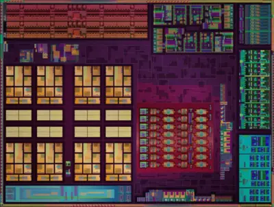
| + | == Die == | ||
| + | {{amd renoir die}} | ||
Latest revision as of 11:30, 23 October 2023
| Edit Values | |
| Ryzen 7 4700U | |
| General Info | |
| Designer | AMD |
| Manufacturer | TSMC |
| Model Number | 4700U |
| Part Number | 100-000000083 |
| Market | Mobile |
| Introduction | January 6, 2020 (announced) January 6, 2020 (launched) |
| Shop | Amazon |
| General Specs | |
| Family | Ryzen 7 |
| Series | 4000 |
| Locked | Yes |
| Frequency | 2,000 MHz |
| Turbo Frequency | 4,100 MHz |
| Clock multiplier | 20 |
| Microarchitecture | |
| ISA | x86-64 (x86) |
| Microarchitecture | Zen 2 |
| Core Name | Renoir |
| Core Family | 23 |
| Core Model | 96 |
| Core Stepping | A1 |
| Process | 7 nm |
| Transistors | 9,800,000,000 |
| Technology | CMOS |
| Die | 156 mm² |
| Word Size | 64 bit |
| Cores | 8 |
| Threads | 8 |
| Max Memory | 64 GiB |
| Multiprocessing | |
| Max SMP | 1-Way (Uniprocessor) |
| Electrical | |
| TDP | 15 W |
| cTDP down | 10 W |
| cTDP up | 25 W |
| Tcase | 0 °C – 105 °C |
| Packaging | |
| Package | FP6 (FC-OBGA) |
| Dimension | 35 mm × 25 mm × 1.38 mm |
| Pitch | 0.65 mm |
| Contacts | 1140 |
Ryzen 7 4700U is a 64-bit octa-core high-end performance x86 mobile microprocessor introduced by AMD in early 2020. Fabricated on TSMC's 7-nanometer process and based on AMD's Zen 2 microarchitecture, the 4700U operates at a base frequency of 2.0 GHz with a TDP of 15 W and a boost frequency of up to 4.1 GHz. This APU supports up to 64 GiB of DDR4-3200 or up to 32 GiB of quad-channel LPDDR4x-4266 memory. This chip integrates Radeon Vega 7 graphics operating at up to 1.6 GHz.
This model supports a configurable TDP-down of 10 W and TDP-up of 25 W.
Cache[edit]
- Main article: Zen 2 § Cache
|
Cache Organization
Cache is a hardware component containing a relatively small and extremely fast memory designed to speed up the performance of a CPU by preparing ahead of time the data it needs to read from a relatively slower medium such as main memory. The organization and amount of cache can have a large impact on the performance, power consumption, die size, and consequently cost of the IC. Cache is specified by its size, number of sets, associativity, block size, sub-block size, and fetch and write-back policies. Note: All units are in kibibytes and mebibytes. |
|||||||||||||||||||||||||||||||||||||
|
|||||||||||||||||||||||||||||||||||||
Memory controller[edit]
This SoC features two memory controllers, each supporting DDR4 or LPDDR4x. This chip supports up to 64 GiB of dual-channel DDR4 memory with data rates of up to 3200 MT/s (51.2 GB/s) or up to 32 GiB of quad-channel LPDDR4x with data rates of up to 4266 MT/s (68.27 GB/s).
|
Integrated Memory Controller
|
||||||||||||
|
||||||||||||
Expansions[edit]
This processor has 16 PCIe lanes, 1x8 designated for a discrete GPU, 1x4 additional lanes for storage (e.g., NVMe), and 1x4 additional lanes reserved for additional peripherals (e.g., WiFi or LTE).
Expansion Options |
|||||
|
|||||
Graphics[edit]
|
Integrated Graphics Information
|
||||||||||||||||||
|
||||||||||||||||||
| [Edit] Zen 2 with Radeon Vega Hardware Accelerated Video Capabilities | |||||
|---|---|---|---|---|---|
| Codec | Encode | Decode | |||
| VP9 8bpc/10bpc | 1080p240 4K 60 FPS | ||||
| MPEG-2 (H.262) 8b | 1080p240 4K 60 FPS |
1080p480 4K 120 FPS | |||
| HEVC (H.265) 8bpc/10bpc | 1080p240 4K 60 FPS |
1080p240 4K 60 FPS | |||
Features[edit]
[Edit/Modify Supported Features]
|
Supported x86 Extensions & Processor Features
|
||||||||||||||||||||||||||||||||||||||||||||||||||||||||||||||||
|
||||||||||||||||||||||||||||||||||||||||||||||||||||||||||||||||
Die[edit]
- Main article: Zen 2 § Die
Renoir microprocessors are fabricated on TSMC's 7-nanometer process. This SoC integrates 9.8 billion transistors on a single 156 mm² monolithic die which includes both the Zen 2 CPU cores along with the Vega GPU and various other additional components.
- 7-nanometer process (N7)
- 9,800,000,000 transistors
- 156 mm² die size
| Has subobject "Has subobject" is a predefined property representing a container construct and is provided by Semantic MediaWiki. | Ryzen 7 4700U - AMD#pcie + |
| base frequency | 2,000 MHz (2 GHz, 2,000,000 kHz) + |
| clock multiplier | 20 + |
| core count | 8 + |
| core family | 23 + |
| core model | 96 + |
| core name | Renoir + |
| core stepping | A1 + |
| designer | AMD + |
| die area | 156 mm² (0.242 in², 1.56 cm², 156,000,000 µm²) + |
| family | Ryzen 7 + |
| first announced | January 6, 2020 + |
| first launched | January 6, 2020 + |
| full page name | amd/ryzen 7/4700u + |
| has advanced vector extensions | true + |
| has advanced vector extensions 2 | true + |
| has amd amd-v technology | true + |
| has amd amd-vi technology | true + |
| has amd sensemi technology | true + |
| has ecc memory support | false + |
| has feature | Advanced Vector Extensions +, Advanced Vector Extensions 2 +, Advanced Encryption Standard Instruction Set Extension + and SenseMI Technology + |
| has locked clock multiplier | true + |
| has x86 advanced encryption standard instruction set extension | true + |
| instance of | microprocessor + |
| integrated gpu | Radeon Vega 7 + |
| integrated gpu designer | AMD + |
| integrated gpu execution units | 7 + |
| integrated gpu max frequency | 1,600 MHz (1.6 GHz, 1,600,000 KHz) + |
| isa | x86-64 + |
| isa family | x86 + |
| l1$ size | 512 KiB (524,288 B, 0.5 MiB) + |
| l1d$ description | 8-way set associative + |
| l1d$ size | 256 KiB (262,144 B, 0.25 MiB) + |
| l1i$ description | 8-way set associative + |
| l1i$ size | 256 KiB (262,144 B, 0.25 MiB) + |
| l2$ description | 8-way set associative + |
| l2$ size | 4 MiB (4,096 KiB, 4,194,304 B, 0.00391 GiB) + |
| l3$ description | 16-way set associative + |
| l3$ size | 8 MiB (8,192 KiB, 8,388,608 B, 0.00781 GiB) + |
| ldate | January 6, 2020 + |
| manufacturer | TSMC + |
| market segment | Mobile + |
| max case temperature | 378.15 K (105 °C, 221 °F, 680.67 °R) + |
| max cpu count | 1 + |
| max memory | 65,536 MiB (67,108,864 KiB, 68,719,476,736 B, 64 GiB, 0.0625 TiB) + |
| max memory bandwidth | 63.581 GiB/s (65,107.346 MiB/s, 68.27 GB/s, 68,270 MB/s, 0.0621 TiB/s, 0.0683 TB/s) + |
| max memory channels | 4 + |
| microarchitecture | Zen 2 + |
| min case temperature | 273.15 K (0 °C, 32 °F, 491.67 °R) + |
| model number | 4700U + |
| name | Ryzen 7 4700U + |
| package | FP6 + |
| part number | 100-000000083 + |
| process | 7 nm (0.007 μm, 7.0e-6 mm) + |
| series | 4000 + |
| smp max ways | 1 + |
| supported memory type | DDR4-2666 + and LPDDR4x-4266 + |
| tdp | 15 W (15,000 mW, 0.0201 hp, 0.015 kW) + |
| tdp down | 10 W (10,000 mW, 0.0134 hp, 0.01 kW) + |
| tdp up | 25 W (25,000 mW, 0.0335 hp, 0.025 kW) + |
| technology | CMOS + |
| thread count | 8 + |
| transistor count | 9,800,000,000 + |
| turbo frequency | 4,100 MHz (4.1 GHz, 4,100,000 kHz) + |
| word size | 64 bit (8 octets, 16 nibbles) + |