| Edit Values | |
| Socket S1g1 | |
| General Info | |
| Designer | AMD |
| Introduction | May 17, 2006 (launched) |
| Market | Mobile |
| Microarchitecture | K8 |
| TDP | 35 W 35,000 mW 0.0469 hp 0.035 kW |
| Package | |
| Name | OPGA-638 |
| Type | Organic Micro Pin Grid Array |
| Contacts | 638 |
| Dimension | 35.0 mm 3.5 cm × 35.0 mm1.378 in 3.5 cm 1.378 in |
| Pitch | 1.27 mm 0.05 in |
| Socket | |
| Name | Socket S1g1 |
| Type | PGA |
Socket S1, specifically S1g1, the first of four revisions, was a low-profile ZIF socket for OPGA-638-packaged AMD mobile microprocessors with an integrated DDR2 memory controller, and the successor to Socket 754 in the mobile segment. Its counterparts are Socket AM2 for desktop processors and Socket F for servers and workstations. For the small form factor desktop, ultrathin mobile, and embedded market AMD developed package ASB1. Socket S1g1 was superseded by Socket S1g2.
Socket S1g1 was used in AMD's second and third mobile platform "Kite" (2006) and "Kite Refresh" (2007). All processors for Socket S1g1 are members of AMD's Family 0Fh with CPU cores based on the K8 microarchitecture.
All revisions of Socket S1 have the same dimensions, however processors for Socket S1g1 appear to be electrically incompatible with all later revisions of this socket.
Contents
Features
- 638-pin lidless micro pin grid array package, 1.27 mm pitch, 26 × 26 pins, 35 × 35 mm, organic substrate, C4 (flip chip) die attachment
- 16 bit HyperTransport 1.0 interface up to 800 MHz, 1600 MT/s, 3.2 GB/s in each direction
- 128 bit DDR2 SDRAM interface up to 400 MHz, PC2-6400 (DDR2-800), 12.8 GB/s
- Up to 2 unbuffered SO-DIMMs, no ECC support
- JEDEC SSTL_1.8
- P-States, multiple ACPI compliant low-power states including C1E with AltVID, AMD PowerNow! technology
- Thermal Controls
- Thermal protection
- Hardware thermal control
- Thermal diode
Chipsets
- AMD M690, M690V, M690E, M690T
- AMD SB600 southbridge
- Mvidia GeForce 7000M, 7150M, southbridge integrated
Processors using Socket S1g1
- "Kite" platform:
- "Kite Refresh" platform:
| List of all Socket S1g1-based Processors | |||||||||||||||||||
|---|---|---|---|---|---|---|---|---|---|---|---|---|---|---|---|---|---|---|---|
| Model | Price | Process | Launched | µarch | Family | Core | C | T | Freq | Turbo | TDP | ||||||||
| Count: 0 | |||||||||||||||||||
Package Diagram
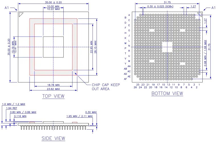
OPGA-638 package dimensions as specified in AMD Publ. #31839. This is part no. 29249 with the chip used for Turion 64 "Richmond" and Sempron "Keene" processors. All dimensions in millimeters.
Socket Outline
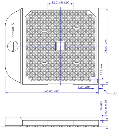
Socket S1 limits as specified in AMD Publ. #31839. Depicted is Foxconn Interconnect Technology Part No. PZ6382A-284S-01F. All dimensions in millimeters.
Pin Map
For differences to other Socket S1 revisions see Socket S1g4.
Pin Description
| Signal | Description |
|---|---|
| CLKIN_H/L | 200 MHz Differential PLL Reference Clock |
| CPU_PRESENT_L | Processor is present, shorted to VSS on the package |
| DBREQ_L, DBRDY | Debug Request/Ready |
| HTREF0, HTREF1 | HyperTransport Compensation Resistor to VSS, VLDT |
| L0_CADIN/OUT_H/L[15:0] | HT Link 0 Differential Command/Address/Data Input/Output |
| L0_CLKIN/OUT_H/L[1:0] | HT Link 0 Differential Clock Input/Output |
| L0_CTLIN_H/L[1:0] | HT Link 0 Differential Control Input/Output |
| LDTSTOP_L | HT Stop Control Input for power management and link width and frequency change |
| MA0/MB0_CLK_H/L[2:1] | DRAM Differential Clock |
| MA0/MB0_CS_L[3:0] | DRAM Chip Select |
| MA0/MB0_ODT[1:0] | DRAM Enable Pin for On Die Termination |
| MA/MB_ADD[15:0] | DRAM Column/Row Address |
| MA/MB_BANK[2:0] | DRAM Bank Address |
| MA/MB_CAS_L | DRAM Column Address Strobe |
| MA/MB_CKE[1:0] | DRAM Clock Enable |
| MA/MB_DATA[63:0] | DRAM Data Bus |
| MA/MB_DM[7:0] | DRAM Data Mask |
| MA/MB_DQS_H/L[7:0] | DRAM Differential Data Strobe |
| MA/MB_RAS_L | DRAM Row Address Strobe |
| MA/MB_WE_L | DRAM Write Enable |
| MEMVREF | DRAM Interface Voltage Reference |
| MEMZP, MEMZN | Compensation Resistor to VSS, VDDIO |
| PROCHOT_L | Processor in HTC-active state input/output |
| PSI_L | Power Status Indicator (low power state) for VDD regulator |
| PWROK | Voltages and CLKIN have reached specified operation |
| RESET_L | Processor Reset |
| RSVD | Reserved |
| SIC, SID | Sideband Temperature Sensor Interface Clock, Data |
| TCK, TDI, TDO, TMS, TRST_L | JTAG interface |
| TEST* | Test signal |
| THERMDA, THERMDC | Thermal Diode Anode, Cathode |
| THERMTRIP_L | Thermal Sensor Trip output |
| VDD | Core power supply |
| VDD_FB_H/L | Differential feedback to VDD regulator |
| VDDA | Filtered PLL supply voltage |
| VDDIO | DRAM I/O ring power supply |
| VDDIO_FB_H/L | Differential feedback to VDDIO regulator |
| VID[5:0] | Voltage ID for VDD regulator |
| VLDT_A/B | HyperTransport I/O ring power supply |
| VSS | Ground |
| VTT | DRAM Termination voltage |
| VTT_SENSE | VTT monitor pin |
References
- "Low-Profile Socket S1 Design Specification", AMD Publ. #31839, Rev. 3.01, April 10, 2007
- "BIOS and Kernel Developer's Guide for AMD NPT Family 0Fh Processors", AMD Publ. #32559, Rev. 3.16, October 31, 2009
- "AMD Turion™ 64 Mobile Technology Product Data Sheet", AMD Publ. #32816, Rev. 3.05, September 10, 2006
- "AMD Turion™ 64 X2 Mobile Technology Dual-Core Processor Product Data Sheet", AMD Publ. #41407, Rev. 3.02, September 10, 2006
- "AMD Athlon™ 64 X2 Dual-Core Processor for Notebooks Product Data Sheet", AMD Publ. #42989, Rev. 3.01, August 2007
- "Revision Guide for AMD NPT Family 0Fh Processors", AMD Publ. #33610, Rev. 3.48, December 13, 2011
See also
| designer | AMD + |
| first launched | May 17, 2006 + |
| instance of | package + |
| market segment | Mobile + |
| microarchitecture | K8 + |
| name | Socket S1g1 + |
| package | OPGA-638 + |
| package contacts | 638 + |
| package length | 35 mm (3.5 cm, 1.378 in) + |
| package pitch | 1.27 mm (0.05 in) + |
| package type | Organic Micro Pin Grid Array + |
| package width | 35 mm (3.5 cm, 1.378 in) + |
| socket | Socket S1g1 + |
| tdp | 35 W (35,000 mW, 0.0469 hp, 0.035 kW) + |


