| Edit Values | |
| Socket AM3 | |
| General Info | |
| Designer | AMD |
| Introduction | February 9, 2009 (launched) |
| Market | Desktop |
| Microarchitecture | K10 |
| TDP | 125 W 125,000 mW 0.168 hp 0.125 kW |
| Package | |
| Name | OPGA-938 |
| Type | Organic Micro Pin Grid Array |
| Contacts | 938 |
| Dimension | 40.0 mm 4 cm × 40.0 mm1.575 in 4 cm 1.575 in |
| Pitch | 1.27 mm 0.05 in |
| Socket | |
| Name | Socket AM3 |
| Type | PGA |
Socket AM3 was the socket for OPGA-938 and OPGA-940-packaged AMD microprocessors with an integrated DDR2/DDR3 memory controller and the successor to Socket AM2+. Socket AM3 targets the desktop segment. Its contemporaries are Socket S1 for mobile processors, Socket C32 and Socket G34 for the server and workstation market. For the small form factor desktop, mobile and embedded market AMD developed package ASB2. Socket AM3 was superseded by Socket AM3+.
Socket AM3 processors use the OPGA-938 package and, supporting both DDR2 and DDR3 SDRAM, are compatible with the earlier Sockets AM2 and AM2+, subject to the motherboard recognizing the CPU and configuring its memory controller for DDR2 mode. These processors are likewise compatible with Socket AM3+. Socket AM3 and AM3+ motherboards use DDR3 SDRAM and configure the processor accordingly. The OPGA-938 package has the same dimensions but is mechanically, due to keying, and electrically incompatible with Socket 939 for processors with a DDR memory controller, and Socket 940 for first generation Opteron processors.
Socket AM3+ processors use the OPGA-940 package and are compatible with Socket AM3, subject to the motherboard recognizing the CPU and the limitations of Socket AM3. The OPGA-940 package for Socket AM2/AM2+ differs from the OPGA-940 package for Socket AM3/AM3+ by keying and electrically. The former carries CPUs requiring DDR2 SDRAM, the latter processors supporting DDR3 SDRAM exclusively. Socket AM2/AM2+ processors are therefore incompatible with Socket AM3.
All processors for Socket AM3 belong to AMD's Family 10h and use the K10 microarchitecture.
Contents
Features
- 938/940-pin lidded micro pin grid array package, 1.27 mm pitch, 31 × 31 pins, 40 × 40 mm, organic substrate
- 16 bit HyperTransport interface
- Generation 1.0 mode up to 1 GHz, 2000 MT/s, 4 Gbyte/s in each direction
- Generation 3.0 mode up to 2.2 GHz, 4400 MT/s, 8.8 Gbyte/s in each direction
- 2 × 64/72 bit DDR2 SDRAM interface (ganged or unganged) up to 533 MHz, PC-8500 (DDR2-1066), 17.0 Gbyte/s
- Up to 4 UDIMMs (2 per channel), up to 4 Gbyte per UDIMM, SEC-DED ECC
- JEDEC SSTL_1.8
- 2 × 64/72 bit DDR3 SDRAM interface (ganged or unganged) up to 667 MHz, PC3-10600 (DDR3-1333), 21.3 Gbyte/s
- Up to 4 UDIMMs (2 per channel), up to 8 Gbyte per UDIMM, SEC-DED ECC
- JEDEC 1.5V
- Mixing of DDR2 and DDR3 or ECC and non-ECC DIMMs is not supported
- P-States; ACPI C0, C1, C1E, S0, S1, S3, S4, S5; dual power planes
- Thermal diode, overtemperature protection
Chipsets
- AMD 700, 800, 900 series
- Nvidia nForce 630a, 980a SLI
Processors using Socket AM3
- AMD Opteron "Suzuka" (4C UP)
- AMD Phenom II X6 "Thuban", X4 "Zosma", X4 (native) "Deneb", X3 "Heka", X2 "Callisto"
- AMD Phenom II XLT
- AMD Athlon II X4 "Propus", X3 "Rana", X2 "Regor"
- AMD Athlon II "Sargas"
- AMD Athlon II XL and XLT
- AMD Sempron X2 "Regor"
- AMD Sempron "Sargas"
| List of all Socket AM3-based Processors | |||||||||||||||||||
|---|---|---|---|---|---|---|---|---|---|---|---|---|---|---|---|---|---|---|---|
| Model | Price | Process | Launched | µarch | Family | Core | C | T | Freq | Turbo | TDP | ||||||||
| Count: 0 | |||||||||||||||||||
Package Diagram
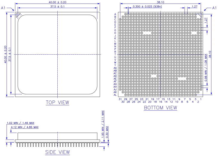
OPGA-938 package. All dimensions in millimeters.
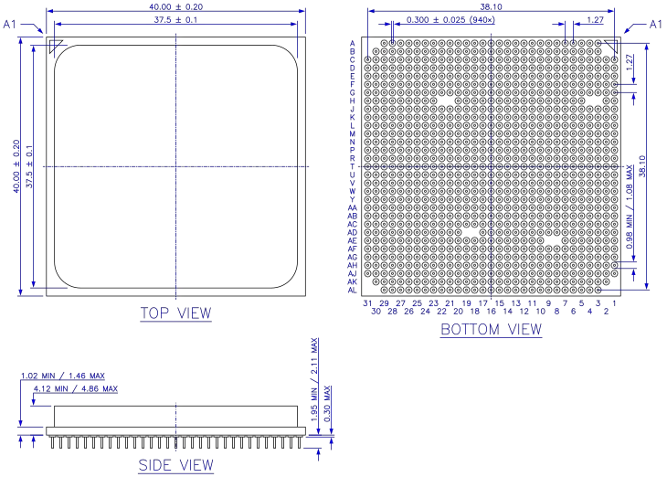
OPGA-940 package for Socket AM3/AM3+. All dimensions in millimeters.
Socket Outline
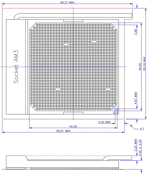
Socket AM3. Note the socket cover has 941 pin holes. Pin B2 is not populated on the OPGA-938 and OPGA-940 package and unconnected on the socket. All dimensions in millimeters.
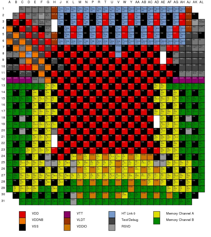
Pin Map
Socket AM2/AM2+/AM3 Differences
| Pin | Socket AM2 | Socket AM2+ | Socket AM3 |
|---|---|---|---|
| AL4 | RSVD | ALERT_L | ALERT_L |
| G5 | RSVD | CORE_TYPE | CORE_TYPE |
| G20 | MA1_CLK_H[1] | MA1_CLK_H[1] | MA_CLK_H[0] |
| G21 | MA1_CLK_L[1] | MA1_CLK_L[1] | MA_CLK_L[0] |
| G19 | MA0_CLK_H[1] | MA0_CLK_H[1] | MA_CLK_H[1] |
| H19 | MA0_CLK_L[1] | MA0_CLK_L[1] | MA_CLK_L[1] |
| U24 | RSVD | RSVD | MA_CLK_H[2] |
| V24 | RSVD | RSVD | MA_CLK_L[2] |
| W26 | RSVD | RSVD | MA_CLK_H[3] |
| W25 | RSVD | RSVD | MA_CLK_L[3] |
| V27 | MA1_CLK_H[0] | MA1_CLK_H[0] | MA_CLK_H[4] |
| W27 | MA1_CLK_L[0] | MA1_CLK_L[0] | MA_CLK_L[4] |
| U27 | MA0_CLK_H[0] | MA0_CLK_H[0] | MA_CLK_H[5] |
| U26 | MA0_CLK_L[0] | MA0_CLK_L[0] | MA_CLK_L[5] |
| AE20 | MA1_CLK_H[2] | MA1_CLK_H[2] | MA_CLK_H[6] |
| AE19 | MA1_CLK_L[2] | MA1_CLK_L[2] | MA_CLK_L[6] |
| AG21 | MA0_CLK_H[2] | MA0_CLK_H[2] | MA_CLK_H[7] |
| AG20 | MA0_CLK_L[2] | MA0_CLK_L[2] | MA_CLK_L[7] |
| C19 | MB1_CLK_H[1] | MB1_CLK_H[1] | MB_CLK_H[0] |
| D19 | MB1_CLK_L[1] | MB1_CLK_L[1] | MB_CLK_L[0] |
| A18 | MB0_CLK_H[1] | MB0_CLK_H[1] | MB_CLK_H[1] |
| A19 | MB0_CLK_L[1] | MB0_CLK_L[1] | MB_CLK_L[1] |
| V31 | RSVD | RSVD | MB_CLK_H[2] |
| W31 | RSVD | RSVD | MB_CLK_L[2] |
| Y31 | RSVD | RSVD | MB_CLK_H[3] |
| Y30 | RSVD | RSVD | MB_CLK_L[3] |
| W29 | MB1_CLK_H[0] | MB1_CLK_H[0] | MB_CLK_H[4] |
| W28 | MB1_CLK_L[0] | MB1_CLK_L[0] | MB_CLK_L[4] |
| U31 | MB0_CLK_H[0] | MB0_CLK_H[0] | MB_CLK_H[5] |
| U30 | MB0_CLK_L[0] | MB0_CLK_L[0] | MB_CLK_L[5] |
| AL19 | MB1_CLK_H[2] | MB1_CLK_H[2] | MB_CLK_H[6] |
| AL18 | MB1_CLK_L[2] | MB1_CLK_L[2] | MB_CLK_L[6] |
| AJ19 | MB0_CLK_H[2] | MB0_CLK_H[2] | MB_CLK_H[7] |
| AK19 | MB0_CLK_L[2] | MB0_CLK_L[2] | MB_CLK_L[7] |
| W30 | RSVD | RSVD | MA_EVENT_L |
| V29 | RSVD | RSVD | MB_EVENT_L |
| AE28 | RSVD | RSVD | MA0_ODT[1] |
| AE27 | RSVD | RSVD | MA1_ODT[1] |
| AF31 | RSVD | RSVD | MB0_ODT[1] |
| AG31 | RSVD | RSVD | MB1_ODT[1] |
| E20 | RSVD | RSVD | MA_RESET_L |
| B19 | RSVD | RSVD | MB_RESET_L |
| F3 | RSVD | RSVD | M_VDDIO_PWRGD |
| F2 | RSVD | PLATFORM_TYPE | |
| AK4 | RSVD | SA[0] | SA[0] |
| E2 | VID[1] | PVIEN/VID[1] | PVIEN/VID[1] |
| E3 | VID[2] | SVD/VID[2] | SVD/VID[2] |
| C1 | VID[3] | SVC/VID[3] | SVC/VID[3] |
| A4 | VDD | VDDNB | VDDNB |
| A6 | VDD | VDDNB | VDDNB |
| B5 | VDD | VDDNB | VDDNB |
| B7 | VDD | VDDNB | VDDNB |
| C6 | VDD | VDDNB | VDDNB |
| C8 | VDD | VDDNB | VDDNB |
| D7 | VDD | VDDNB | VDDNB |
| D9 | VDD | VDDNB | VDDNB |
| E10 | VDD | VDDNB | VDDNB |
| E8 | VDD | VDDNB | VDDNB |
| F11 | VDD | VDDNB | VDDNB |
| F9 | VDD | VDDNB | VDDNB |
| G10 | VDD | VDDNB | VDDNB |
| G12 | VDD | VDDNB | VDDNB |
| G4 | RSVD | VDDNB_FB_H | VDDNB_FB_H |
| G3 | RSVD | VDDNB_FB_L | VDDNB_FB_L |
| A12 | VTT | VTT | VDDR |
| AG12 | VTT | VTT | VDDR |
| AH12 | VTT | VTT | VDDR |
| AJ12 | VTT | VTT | VDDR |
| AK12 | VTT | VTT | VDDR |
| AL12 | VTT | VTT | VDDR |
| B12 | VTT | VTT | VDDR |
| C12 | VTT | VTT | VDDR |
| D12 | VTT | VTT | VDDR |
| E12 | VTT_SENSE | VTT_SENSE | VDDR_SENSE |
| B2 | VOID | VOID | NP/RSVD |
| AE7 | VOID | VOID | NP/VSS |
| H20 | VOID | VOID | NP/VSS |
| AE9 | VSS | VSS | VOID |
| H22 | VSS | VSS | VOID |
Pin Description
| Signal | Description |
|---|---|
| ALERT_L | Programmable pin that can indicate different events, including a SB-TSI interrupt |
| CLKIN_H/L | 200 MHz Differential PLL Reference Clock |
| CORE_TYPE | Indicates that the processor is capable of split core and northbridge voltage plane operation |
| CPU_PRESENT_L | Processor is present, shorted to VSS on the package |
| DBREQ_L, DBRDY | Debug Request/Ready |
| HTREF0, HTREF1 | HyperTransport Compensation Resistor to VSS, VLDT |
| L0_CADIN/OUT_H/L[15:0] | HT Link 0 Differential Command/Address/Data Input/Output |
| L0_CLKIN/OUT_H/L[1:0] | HT Link 0 Differential Clock Input/Output |
| L0_CTLIN_H/L[1:0] | HT Link 0 Differential Control Input/Output |
| LDTSTOP_L | HT Stop Control Input for power management and link width and frequency change |
| MA/MB_ADD[15:0] | DRAM Column/Row Address |
| MA/MB_BANK[2:0] | DRAM Bank Address |
| MA/MB_CAS_L | DRAM Column Address Strobe |
| MA/MB_CHECK[7:0] | DRAM ECC Bits |
| MA/MB_CKE[1:0] | DRAM Clock Enable |
| MA/MB_CLK_H/L[7:0] | DRAM Differential Clock |
| MA/MB_DATA[63:0] | DRAM Data Bus |
| MA/MB_DM[8:0] | DRAM Data Mask |
| MA/MB_DQS_H/L[8:0] | DRAM Differential Data Strobe |
| MA/MB_EVENT_L | DRAM Thermal Event Status |
| MA/MB_RAS_L | DRAM Row Address Strobe |
| MA/MB_RESET_L | DRAM Reset Pin for Suspend-to-RAM Power Management Mode |
| MA/MB_WE_L | DRAM Write Enable |
| MA0/MA1/MB0/MB1_CS_L[1:0] | DRAM Chip Select |
| MA0/MA1/MB0/MB1_ODT[1:0] | DRAM Enable Pin for On Die Termination |
| M_VDDIO_PWRGD | Not supported |
| M_VREF | DRAM Interface Voltage Reference |
| M_ZP, M_ZN | Compensation Resistor to VSS, VDDIO |
| NP/RSVD | Pin is not populated on OPGA-938 and OPGA-940 package, unconnected on Socket AM3 |
| NP/VSS | Pin is not populated on OPGA-938 package, connected to ground on OPGA-940 and Socket AM3 |
| PROCHOT_L | Processor in HTC-active state input/output |
| PSI_L | Power Status Indicator (low power state) for VDD regulator |
| PVIEN/VID[1] | Prior to PWROK assertion signals to the processor whether the platform supports PVI or SVI operation |
| PWROK | Voltages and CLKIN have reached specified operation |
| RESET_L | Processor Reset |
| RSVD | Reserved |
| SA[0] | Sideband interface (APML/SBI/SMBus) address selection |
| SIC, SID | Sideband Temperature Sensor Interface Clock/Data |
| SVC/VID[3] | Serial VID Interface Clock |
| SVD/VID[2] | Serial VID Interface Data |
| TCK, TDI, TDO, TMS, TRST_L | JTAG interface |
| TEST* | Test signal |
| THERMDA, THERMDC | Thermal Diode Anode, Cathode |
| THERMTRIP_L | Thermal Sensor Trip output |
| VDDA | Filtered PLL supply voltage |
| VDDIO | DRAM I/O ring power supply |
| VDDIO_FB_H/L | Differential feedback to VDDIO regulator |
| VDDNB | Northbridge power supply |
| VDDNB_FB_H/L | Differential feedback to VDDNB regulator |
| VDDR | VDDR power supply |
| VDDR_SENSE | VDDR voltage monitor pin |
| VDD | Core power supply |
| VDD_FB_H/L | Differential feedback to VDD regulator |
| VID[5:0] | Voltage ID (PVI) for VDD regulator |
| VLDT_A/B | HyperTransport I/O ring power supply |
| VOID | Missing pins and pin holes for mechanical keying |
| VSS | Ground |
References
- "Socket AM3 Design Specification", AMD Publ. #40523, Rev. 1.06, April 2010
- "Socket AM3 Processor Functional Data Sheet", AMD Publ. #40778, Rev. 1.13, January 2009
- "BIOS and Kernel Developer’s Guide (BKDG) for AMD Family 10h Processors", AMD Publ. #31116, Rev. 3.48, April 22, 2010
- "Family 10h AMD Opteron™ Processor Product Data Sheet", AMD Publ. #40036, Rev. 3.04, June 2010
- "Family 10h AMD Phenom™ II Processor Product Data Sheet", AMD Publ. #46878, Rev. 3.04, February 2009
- "Family 10h AMD Athlon™ II Processor Product Data Sheet", AMD Publ. #49457, Rev. 3.05, February 2011
- "Revision Guide for AMD Family 10h Processors", AMD Publ. #41322, Rev. 3.92, March 2012
See also
| designer | AMD + |
| first launched | February 9, 2009 + |
| instance of | package + |
| market segment | Desktop + |
| microarchitecture | K10 + |
| name | Socket AM3 + |
| package | OPGA-938 + |
| package contacts | 938 + |
| package length | 40 mm (4 cm, 1.575 in) + |
| package pitch | 1.27 mm (0.05 in) + |
| package type | Organic Micro Pin Grid Array + |
| package width | 40 mm (4 cm, 1.575 in) + |
| socket | Socket AM3 + |
| tdp | 125 W (125,000 mW, 0.168 hp, 0.125 kW) + |


