From WikiChip
Socket 940 - AMD
| Edit Values | |
| Socket 940 | |
| General Info | |
| Designer | AMD |
| Introduction | April 22, 2003 (launched) |
| Market | Server |
| Microarchitecture | K8 |
| TDP | 110 W 110,000 mW 0.148 hp 0.11 kW |
| Package | |
| Name | CPGA-940 |
| Type | Ceramic Pin Grid Array |
| Contacts | 940 |
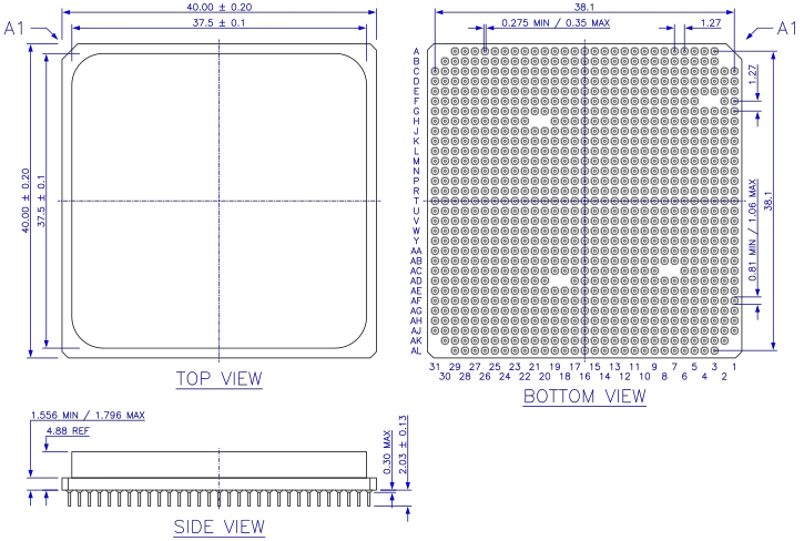
| Dimension | 40.0 mm 4 cm × 40.0 mm1.575 in 4 cm 1.575 in |
| Pitch | 1.27 mm 0.05 in |
| Socket | |
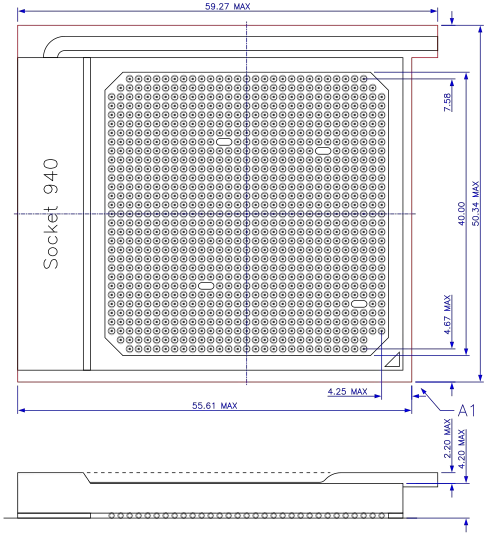
| Name | Socket 940 |
| Type | PGA |
Socket 940 was the socket for µCPGA-940 and µOPGA-940-packaged AMD Opteron and Athlon 64 FX microprocessors, AMD's first generation of server and workstation processors, based on the K8 microarchitecture. Socket 940 was superseded by Socket F.
The µOPGA-940 package for Socket 940 is mechanically (due to keying) and electrically incompatible with the 940-pin Socket AM2.
Contents
Features
- 940-pin lidded micro pin grid array, 1.27 mm pitch, 31 × 31 pins, 40 × 40 mm, ceramic or organic substrate
- 1.15 - 1.55 V supply voltage, 110 W TDP
- Three (desktop processors one) 16 bit HyperTransport interfaces
- Up to 800 MHz, 1600 MT/s, 3.2 Gbyte/s in each direction
- Up to 1000 MHz, 2000 MT/s, 4.0 Gbyte/s in each direction (Rev. E and later)
- One coherent link on dual processor models 2xx
- Three coherent links on multiprocessor models 8xx
- 128/144 bit DDR SDRAM interface up to 166 MHz, PC-2666 (DDR-333), 5.3 Gbyte/s
- 128/144 bit DDR SDRAM interface up to 200 MHz, PC-3200 (DDR-400), 6.4 Gbyte/s (Rev. C0 and later)
- Up to 8 RDIMMs, up to 4 Gbyte per DIMM, SEC-DED ECC
- Chip Kill ECC (server/workstation models)
- P-States, ACPI C1 (Halt), S1 (Stop Grant), S3 (Core & HT power down), S5 (all power off)
- Thermal diode, overtemperature protection
Chipsets
- AMD 8000 series
- Nvidia nForce3 Pro250, nForce Professional 2200
Processors using Socket 940
- Athlon 64 FX-51/53 codename "SledgeHammer"
- AMD Opteron 1xx/2xx/8xx "SledgeHammer" (130 nm; Rev. B3, C0, CG; CPGA-940)
- AMD Opteron 1xx/2xx/8xx "Venus", "Troy", "Athens" (90 nm; Rev. D4, E4; OPGA-940)
- AMD Opteron 1xx/2xx/8xx dual core "Denmark", "Italy", "Egypt" (90 nm; Rev. E1, E6; OPGA-940)
| List of all Socket 940-based Processors | |||||||||||||||||||
|---|---|---|---|---|---|---|---|---|---|---|---|---|---|---|---|---|---|---|---|
| Model | Price | Process | Launched | µarch | Family | Core | C | T | Freq | Turbo | TDP | ||||||||
| Count: 0 | |||||||||||||||||||
Package Diagram
CPGA-940 package. All dimensions in millimeters.
Socket Outline
All dimensions in millimeters.
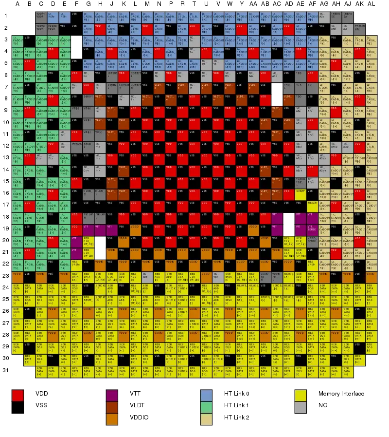
Pin Map
Notes:
- HT Link 1 and 2 are only available on server/workstation processors, NC on desktop processors.
- VLDT is referenced as a unified plane for desktop processors.
- Pin AK2 PRESENCE_DET is only used for server/workstation processors.
References
- "AMD Functional Data Sheet, 940 Pin Package", AMD Publ. #31412
- "AMD Socket 940 Design Specification", AMD Publ. # 25766
- "AMD Opteron™ Processor Product Data Sheet", AMD Publ. #23932
- "AMD Athlon™ 64 FX Product Data Sheet", AMD Publ. #30431
- Keltcher, Chetana N, et al. "The AMD Opteron Processor for Multiprocessor Servers", IEEE Micro 23(2):66–76, March 2003
See also
Facts about "Socket 940 - AMD"
| designer | AMD + |
| first launched | April 22, 2003 + |
| instance of | package + |
| market segment | Server + |
| microarchitecture | K8 + |
| name | Socket 940 + |
| package | CPGA-940 + |
| package contacts | 940 + |
| package length | 40 mm (4 cm, 1.575 in) + |
| package pitch | 1.27 mm (0.05 in) + |
| package type | Ceramic Pin Grid Array + |
| package width | 40 mm (4 cm, 1.575 in) + |
| socket | Socket 940 + |
| tdp | 110 W (110,000 mW, 0.148 hp, 0.11 kW) + |


