| Edit Values | |
| Bulldozer µarch | |
| General Info | |
| Arch Type | CPU |
| Designer | AMD |
| Manufacturer | AMD |
| Introduction | October 12, 2011 |
| Process | 32 nm |
| Instructions | |
| ISA | x86-64 |
| Succession | |
Bulldozer was the microarchitecture developed by AMD as a successor to K10. Bulldozer was superseded by Piledriver in 2012.
Architecture
Bulldozer introduced the concept of Clustered MultiThreading (CMT) to the AMD64 architecture. In CMT, major functional units are shared between groups of integer units to allow manufacturers to lie about how many cores the chips have. Other CMT implementations include the UltraSPARC-T1, codenamed Niagara, which shared a single FPU between many small integer units, each of which also implemented four-way SMT. Overall, Bulldozer marked a major and ambitious departure from AMD's previous designs - and not a very successful one.
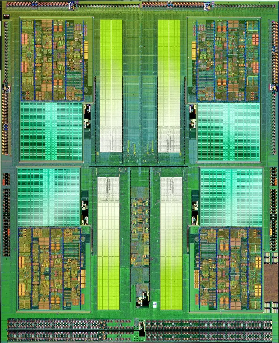
Bulldozer shared one 4-pipe FPU, one L1 I-cache, one set of branch-prediction hardware, one 4-way instruction decoder, and the L2 unified cache between a pair of integer units, referred to by AMD as a module. In the FX-8100 series CPUs, four modules were bundled together with a shared L3 cache, to make an 4-core CPU that was incorrectly marketed as an 8-core CPU for the AM3+ socket. Versions advertised as having four or six cores were also sold by disabling one or two faulty modules; an individual integer unit within a module could not be salvaged through die-harvesting. The Bulldozer core was not used in an APU design, but its successors were.
Pre-release marketing by AMD indicated that the hardware dedicated to each integer unit would include four "integer pipelines", which were each initially assumed by many to be functionally equivalent to the three integer pipelines in K7, K8 and K10. Each integer unit would also have its own level 1 data cache. It was later revealed, however, that only two of the pipelines per integer unit were ALUs, with the other two being AGUs associated with memory loads and stores. Worse, Bulldozer's AGUs could not be used to execute the more complex forms of the LEA (Load Effective Address) instruction efficiently because they had no connection to the result bus, so these instructions had to be cracked for multiple passes through an ALU instead. Effectively, Bulldozer was better described as having two "integer pipelines" and two load-store units per core.
Each of the three "integer pipelines" of K7, K8 and K10 included both an ALU and an AGU for a total of three of each, so Bulldozer (with only two of each) actually had a 33% reduction in integer throughput per integer unit per clock relative to its immediate predecessor, instead of the 33% increase (ie. four of each) that AMD marketing had implied. This had an all-too-predictable effect on integer performance.
The shared FPU was considerably beefed up from K10's, with two FMAC pipelines - capable of executing adds, multiplies, and the new fused-multiply-add (FMA) instructions - and two additional pipelines for other FPU-related operations. In principle, even with both integer units heavily using the shared FPU, this increased capability should have retained rough parity in throughput per integer unit per clock with K10. It could fairly be claimed that this FPU was Bulldozer's best feature.
The four-way instruction decoder, along with the branch predictor, instruction fetcher, and L1 I-cache, could be dedicated to one integer unit if the other integer unit was in sleep mode. Otherwise, they would each dedicate themselves to alternate integer units on successive cycles, effectively halving the fetch and decode bandwidth observed by each integer unit. The decoder was capable of handling four single-op instructions, one double-op and two single-op, or up to four ops from a microcoded instruction, per cycle. Two consecutive double-op instructions had to be decoded in separate cycles. These limitations proved to have a significant effect on performance.
Other differences from K10 lay in the cache hierarchy. The L1 I-cache, which as previously mentioned was now shared between two integer units, was still 64KB and 2-way set-associative, which quickly proved to be a bottleneck when running heterogeneous workloads, because code running on one integer unit would repeatedly evict that required by the other. The L1 D-cache was sharply reduced in size to 16KB and became write-through instead of write-back. Cache and memory latencies were found to be much higher than in K10, which was particularly disappointing since K8 and K10 had made a point of having low latencies with their on-die memory controllers.
Benchmarks quickly demonstrated that, despite Bulldozer's high clock speeds (an overclocking marketing stunt reached 8GHz on LN2) and correspondingly high power consumption, its overall performance was generally no better and often worse than K10. Some aspects of this improved slightly with better OS support, but there were fundamental problems that no mere software tweaks could overcome. Compared to Bulldozer's immediate competitor, Sandy Bridge, the advantage was clearly with the latter, especially for games which, at the time, rarely used more than two or three threads effectively and thrived on low memory latency.
Die Shot
All Bulldozer Chips
| Bulldozer Chips | ||||||
|---|---|---|---|---|---|---|
| Model | Family | Core | Launched | Power Dissipation | Freq | Max Mem |
| Count: 0 | ||||||
See also
| codename | Bulldozer + |
| designer | AMD + |
| first launched | October 12, 2011 + |
| full page name | amd/microarchitectures/bulldozer + |
| instance of | microarchitecture + |
| instruction set architecture | x86-64 + |
| manufacturer | AMD + |
| microarchitecture type | CPU + |
| name | Bulldozer + |
| process | 32 nm (0.032 μm, 3.2e-5 mm) + |
