Semiconductor & Computer Engineering
From WikiChip
Difference between revisions of "User talk:Dahaka88"
m (→Die sizes) |
m (→Die sizes) |
||
| Line 31: | Line 31: | ||
:::https://i.imgur.com/fb4kFYB.png this is real die, right side "small mobile cpu", | :::https://i.imgur.com/fb4kFYB.png this is real die, right side "small mobile cpu", | ||
:::https://cdn.arstechnica.net/wp-content/uploads/2017/10/AMD-Ryzen-processor-with-Radeon-Vega-Graphics_Die-Shot.jpg and this is die picture AMD provided, AMD narrowed its width to make it look better for marketing, so I calculated Ryzen APU dimensions according to "imgur" image which is die is physical, so I think it is reliable for calculation too. Of course assuming "209.78 mm2" is correct for Ryzen APU die size. | :::https://cdn.arstechnica.net/wp-content/uploads/2017/10/AMD-Ryzen-processor-with-Radeon-Vega-Graphics_Die-Shot.jpg and this is die picture AMD provided, AMD narrowed its width to make it look better for marketing, so I calculated Ryzen APU dimensions according to "imgur" image which is die is physical, so I think it is reliable for calculation too. Of course assuming "209.78 mm2" is correct for Ryzen APU die size. | ||
| + | :::https://www.pcgamesn.com/sites/default/files/AMD-Raven-Ridge-Header.png this is how Ryzen APU die looks on physical die, much wider than marketing die photo. | ||
Revision as of 11:03, 17 December 2017
Die sizes
Hello Dahaka88, You've recently added a number of die dimensions to a number of microarchitectures such as Zen, Skylake, and Coffee Lake. In an effort to ensure accuracy on WikiChip, I'm wondering where did those dimensions come from? Thanks --David (talk) 19:56, 15 December 2017 (EST)
- The die dimensions are estimated through knowing die size (Xmm2) and physical die height and width relative each other, I will give you "Zen-Ryzen" die example;
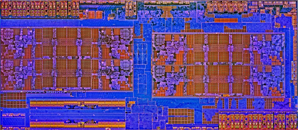
- Ryzen Die Size 213mm2 which is AMD's number, so I assumed it is correct, then I took the picture of die from the wikichip, :https://en.wikichip.org/w/images/thumb/3/3f/amd_zen_octa-core_die_shot.png/950px-amd_zen_octa-core_die_shot.png
- and actual die shot after the delid of the Ryzen CPU,
- https://farm5.static.flickr.com/4353/35620962953_8a12c79f69_b.jpg
- https://www.overclockingmadeinfrance.com/wp-content/uploads/2017/09/RyZen-Die-Shot-3.jpg
- and I measured the width and height by pixels, (2nd picture 1024x448 pixels flickr one),
- 1024/448 = 2,2857~ so wide side is "2,2857a" narrow side is "1a"
- so mathematical equal of 213mm2 is 2,2857a X 1a = 213, 213/2,2857 = a x a = 93,188~ so a = 9,6534~ then multiply a with 2,2857 and 1 for getting dimensions
- ~22,06 x 9,65 = 212.9 the dimensions I got, of course actual dimension require direct measurement, but mathematically this is pretty close "estimated" die size dimension, :also thats why I used "~" symbol to mention that. I hope that helps how I did this estimated die sizes. — Preceding unsigned comment added by Dahaka88 (talk • contribs)
- I see alright. Part of the reason I was asking was because AMD refused to give us exact dimensions. The two die areas we have listed I personally confirmed with AMD, so those are correct. BTW a Zen Zeppelin is actually 212.97 mm2 according to my notes from Hot Chips. You might want to make sure the ratio of your dimensions match the ratio of the images (except for some images like the Skylake server dies, I think the aspect ratio of that image is off). --David (talk) 22:38, 16 December 2017 (EST)
- https://farm5.static.flickr.com/4353/35620962953_8a12c79f69_b.jpg
- https://www.overclockingmadeinfrance.com/wp-content/uploads/2017/09/RyZen-Die-Shot-3.jpg
- These two pictures is physical picture of the Ryzen die after the delid of the cpu thats why I used the "flickr" picture, instead of die image AMD provided, I was suspicious about image "distortion" too.
- https://www.flickr.com/photos/130561288@N04/36123709160/in/album-72157650403404920/
- here is another one taken picture of the "real" ryzen die. You can see the sides of the die "glue" cracks of the photo.
- If AMD refuses to share die dimensions then we will calculate, they cannot stop us from that :)
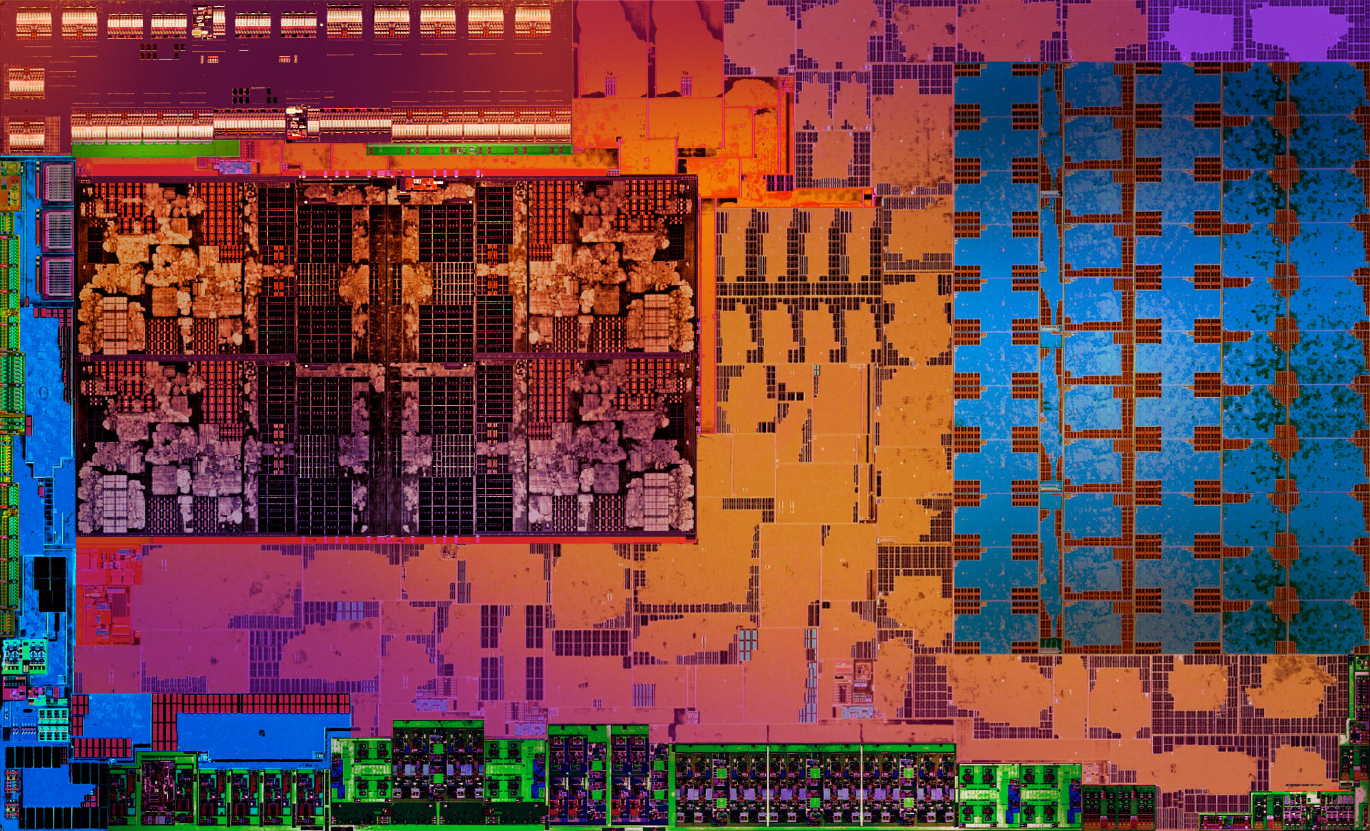
- Also I was suspicious about Ryzen APU die shot it was kinda off to me when I look at "real" die of Ryzen APU at this image
- https://i.imgur.com/fb4kFYB.png this is real die, right side "small mobile cpu",
- https://cdn.arstechnica.net/wp-content/uploads/2017/10/AMD-Ryzen-processor-with-Radeon-Vega-Graphics_Die-Shot.jpg and this is die picture AMD provided, AMD narrowed its width to make it look better for marketing, so I calculated Ryzen APU dimensions according to "imgur" image which is die is physical, so I think it is reliable for calculation too. Of course assuming "209.78 mm2" is correct for Ryzen APU die size.
- https://www.pcgamesn.com/sites/default/files/AMD-Raven-Ridge-Header.png this is how Ryzen APU die looks on physical die, much wider than marketing die photo.