Semiconductor & Computer Engineering
From WikiChip
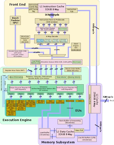
File:skylake block diagram.svg

Size of this PNG preview of this SVG file: 473 × 599 pixels. Other resolution: 189 × 240 pixels.
Original file (SVG file, nominally 991 × 1,255 pixels, file size: 136 KB)
Summary[edit]
| Description |
My own drawing of Intel's Skylake microarchitecture; block diagram. | ||
|---|---|---|---|
| Source |
Own Work. | ||
| Date |
2016 | ||
| Author |
At32Hz | ||
| Permission |
|

File history
Click on a date/time to view the file as it appeared at that time.
| Date/Time | Thumbnail | Dimensions | User | Comment | |
|---|---|---|---|---|---|
| current | 00:01, 6 July 2022 | | 991 × 1,255 (136 KB) | David (talk | contribs) | fixed decoder |
| 23:28, 8 September 2017 |  | 991 × 1,255 (140 KB) | At32Hz (talk | contribs) | ||
| 02:33, 13 July 2017 |  | 991 × 1,255 (140 KB) | David (talk | contribs) | slightly bigger L3 bandwidth label | |
| 04:09, 26 June 2017 |  | 960 × 1,255 (140 KB) | David (talk | contribs) | small correction | |
| 06:58, 20 June 2017 |  | 960 × 1,255 (140 KB) | At32Hz (talk | contribs) | corrected lines that moved | |
| 06:53, 20 June 2017 |  | 960 × 1,255 (140 KB) | At32Hz (talk | contribs) | slight adjustment | |
| 15:08, 6 May 2017 |  | 920 × 1,255 (141 KB) | At32Hz (talk | contribs) | corrected bus line | |
| 15:06, 6 May 2017 |  | 920 × 1,255 (141 KB) | At32Hz (talk | contribs) | ||
| 10:06, 6 May 2017 |  | 920 × 1,255 (141 KB) | At32Hz (talk | contribs) | typo | |
| 00:45, 6 May 2017 |  | 920 × 1,255 (141 KB) | At32Hz (talk | contribs) | arrows | |
| 20:37, 5 May 2017 |  | 920 × 1,255 (143 KB) | At32Hz (talk | contribs) | I think this is a feature complete diagram at this point. am I missing anything? | |
| 22:25, 28 April 2017 |  | 913 × 1,122 (125 KB) | At32Hz (talk | contribs) | added more details; almost feature complete | |
| 15:03, 28 April 2017 |  | 913 × 1,122 (118 KB) | At32Hz (talk | contribs) | various modifications | |
| 00:17, 17 April 2017 |  | 907 × 1,147 (100 KB) | At32Hz (talk | contribs) | correctly adjusted the decode structure | |
| 15:05, 16 January 2017 |  | 850 × 1,075 (86 KB) | At32Hz (talk | contribs) | Corrected Port 4, it was incorrectly labeled as Store Address where it is actually a Store Data port. | |
| 11:44, 2 May 2016 |  | 850 × 1,075 (91 KB) | At32Hz (talk | contribs) | correct text outside of the DSB box; arrow not showing for port 1 | |
| 10:07, 2 May 2016 |  | 850 × 1,075 (91 KB) | At32Hz (talk | contribs) | My own drawing of Intel's {{intel|Skylake}} microarchitecture; block diagram. |
- You cannot overwrite this file.
File usage
The following 3 pages link to this file: