(→Industry) |
|||
| Line 23: | Line 23: | ||
! colspan="2" | [[Intel]] !! colspan="2" | Common Platform<info>[[IBM]] / [[GlobalFoundries]] / [[AMD]] / [[Freescale]] / [[STMicroelectronics]] / [[Toshiba]] / CNSE</info> | ! colspan="2" | [[Intel]] !! colspan="2" | Common Platform<info>[[IBM]] / [[GlobalFoundries]] / [[AMD]] / [[Freescale]] / [[STMicroelectronics]] / [[Toshiba]] / CNSE</info> | ||
|- style="text-align: center;" | |- style="text-align: center;" | ||
| − | | colspan="2" | P1270 || colspan="2" | | + | | colspan="2" | P1270 (CPU) / P1271 (SoC) || colspan="2" | |
|- style="text-align: center;" | |- style="text-align: center;" | ||
| colspan="2" | 2011 || colspan="2" | 2012 | | colspan="2" | 2011 || colspan="2" | 2012 | ||
| Line 33: | Line 33: | ||
| 60 nm || colspan="3" rowspan="3" style="text-align: center;" | N/A | | 60 nm || colspan="3" rowspan="3" style="text-align: center;" | N/A | ||
|- | |- | ||
| − | | | + | | 8 nm |
|- | |- | ||
| − | | | + | | 34 nm |
|- | |- | ||
| 90 nm || 0.80x || 100 nm || 0.79x | | 90 nm || 0.80x || 100 nm || 0.79x | ||
| Line 50: | Line 50: | ||
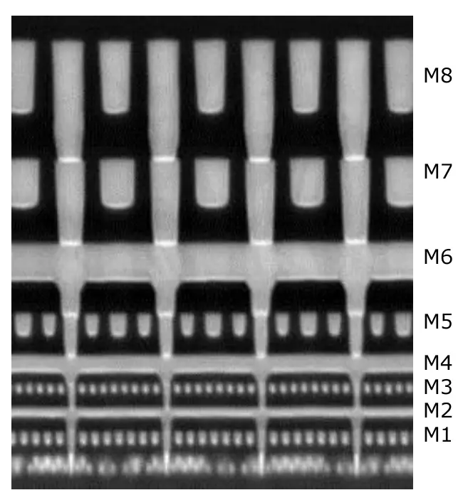
{| class="wikitable collapsible collapsed" | {| class="wikitable collapsible collapsed" | ||
|- | |- | ||
| − | ! colspan=" | + | ! colspan="7" | Intel 22nm SoC Interconnect Design Rules |
|- | |- | ||
| − | ! Layer !! Pitch !! Process !! Dielectric Materials !! [[CPU]] !! [[SoC]] | + | ! Layer !! Pitch !! Process !! Dielectric Materials !! [[CPU]] !! [[SoC]] || Image |
|- | |- | ||
| − | | Fin || 60 nm || - || - || Fin || Fin | + | | Fin || 60 nm || - || - || Fin || Fin || rowspan="9" | [[File:intel 22nm rules.png]] |
|- | |- | ||
| Contact || 90 nm || SAC || - || Contact || Contact | | Contact || 90 nm || SAC || - || Contact || Contact | ||
| Line 72: | Line 72: | ||
| MT - TOP || 14 µm || Plate Up || Polymer || M9 || Top Metal | | MT - TOP || 14 µm || Plate Up || Polymer || M9 || Top Metal | ||
|} | |} | ||
| + | |||
== Find models == | == Find models == | ||
{{#ask: | {{#ask: | ||
Revision as of 08:57, 16 September 2016
The 22 nanometer (22 nm) lithography process is a full node semiconductor manufacturing process following the 28 nm process stopgap. The term "22 nm" is simply a commercial name for a generation of a certain size and its technology, as opposed to gate length or half pitch. Commercial integrated circuit manufacturing using 22 nm process began in 2008 for memory and 2012 for MPUs. This technology was replaced by with 20 nm process (HN) in 2014 and 16 nm process (FN) in late 2015.
Contents
Industry
The 22 nm became Intel's first generation of Tri-gate FinFET transistors and the first such transistor on the market. This process became 3rd generation high-k + metal gate transistors for Intel. Those transistors were not used in IBM's process
| Fab |
|---|
| Process Name |
| 1st Production |
| Wafer |
| |
| Fin Pitch |
| Fin Width |
| Fin Height |
| Contacted Gate Pitch |
| Interconnect Pitch (M1P) |
| SRAM bit cell (HP) |
| SRAM bit cell (HD) |
| DRAM bit cell |
| Intel | Common Platform | ||||
|---|---|---|---|---|---|
| P1270 (CPU) / P1271 (SoC) | |||||
| 2011 | 2012 | ||||
| 300mm | |||||
| Value | 32 nm Δ | Value | 32 nm Δ | ||
| 60 nm | N/A | ||||
| 8 nm | |||||
| 34 nm | |||||
| 90 nm | 0.80x | 100 nm | 0.79x | ||
| 80 nm | 0.71x | 80 nm | ?x | ||
| 0.1080 µm2 | 0.63x | 0.1 µm2 | 0.67x | ||
| 0.092 µm2 | ?x | ||||
| 0.026 µm2 | 0.67x | ||||
Design Rules
| Intel 22nm SoC Interconnect Design Rules | ||||||
|---|---|---|---|---|---|---|
| Layer | Pitch | Process | Dielectric Materials | CPU | SoC | Image |
| Fin | 60 nm | - | - | Fin | Fin | 
|
| Contact | 90 nm | SAC | - | Contact | Contact | |
| M1 | 90 nm | SAV | ULK CDO | M1 | M1 | |
| MT - 1x | 80 nm | SAV | ULK CDO | M2/M3 | 2-6 layers | |
| MT - 1.4x | 112 nm | SAV | ULK CDO | M4 | Semi-global | |
| MT - 2x | 160 nm | SAV | ULK CDO | M5 | Semi-global | |
| MT - 3x | 240 nm | SAV | ULK CDO | M6 | Global Routing | |
| MT - 4x | 320 nm 360 nm |
Via First | LK CDO | M7/M8 | Global Routing | |
| MT - TOP | 14 µm | Plate Up | Polymer | M9 | Top Metal | |
Find models
Click to browse all 22 nm MPU models
22 nm Microprocessors
This list is incomplete; you can help by expanding it.
Click to browse all 22 nm MPU models
22 nm System on Chips
This list is incomplete; you can help by expanding it.
22 nm Microarchitectures
- Intel:
This list is incomplete; you can help by expanding it.
 Semiconductor lithography processes technology